Verification of Withstand Capability for Very Fast Transients of a 200 MVA, 500 kV GSU-Transformer by Modelling and Testing
Authors
A. RABEL - Siemens AG Austria, Transformers Research, Weiz, Austria
J.J. ZHOU - Siemens China, Transformers Research, Jinan, China

Summary
Transformers in the network are often exposed to voltage stresses, that are different from the im-pulses during the factory assessment tests (FAT). In many cases transformers can withstand these voltages. In combination with Gas-insulated switch gears (GIS) it is typical, that these voltages are characterized by a very high steepness in combination with a short duration time, called very fast transients (VFT). Since for VFT voltages the difference to the FAT is remarkable, customers ask for an extended proof of the withstand capability.
It is also clear, that customers are doing own system studies. On the one hand to get more detailed knowledge about voltage stresses to be expected at switching events and fault events, on the other hand it is important to consider these results when doing the specification for transformers connect to GIS.
To cover these requirements, a step by step approach was followed. Starting with providing simpli-fied transformer models, calculating the frequency response, based on the manufacturers white box model. These models are delivered to the customer. Resonance frequencies are derived, and the safety margins as well a proof for acceptable resonant voltages a the HV terminal is given.
Next the proof the withstand capability for voltage stresses at energisation, inductive opening, re-ignitions and disconnecting events is done. Due to the content of very high frequencies in the signals –going up to 5 MHz – it is necessary to use proper models during the transformers design process.Turn wise models of the transformer windings provide a sufficient resolution for the required fre-quency range (>10 MHz). The use of turn wise models of the transformer’s windings are mandatory.
It is a challenge, that a transformer can reliable withstand the VFT voltages. The withstand capability is proven by numerical simulation as well as by a special test. In the test sequence a very steep chop-ping, by applying a special SF6 chopping device, with customer specified voltage levels, finally suc-cessfully proofed the transformers withstand capability for VFT.
Keywords
Power Transformer, VFT, Transformer Modelling, GIS, Transformer Testing, insulation withstand1. Introduction
Power transformers, in the electrical power system in combination with Gas Insulated Switch gears (GIS), are exposed to special transient voltages. These special voltages are not covered by actual standards. They are characterized by a very steep front wave and high oscillation frequency. The rise time (TR) of such a wave is in the range of some nanoseconds (5 to 20 ns) and the peak value is about 1.5 and 2.5 p.u. of rated operating voltage. The frequencies are in the range up to 5 to 10 MHz [3][4]. In the literature, some authors indicate some transformer failures caused by Very Fast Transients (VFT).
2. Challenge
A conventional large power transformer is designed to withstand standard lightning impulses, Full Wave (FW), Chopped Wave (CW) and Switching Impulse (SIL). Modelling and behaviour of trans-formers for this range (< 1MHz) is in the meantime well described in CIGRE brochures [1]. For very fast transients (VFT) no standard is available yet. In order to ensure, that a transformer can withstand these transients, separate requirements have to be specified by the customers.
As a first step a numerical check by calculation for reference waveshapes with as Rise Time (TR) / Tail Time (TT ) of 10ns±50% / 165ns±60% and a level of 2 p.u. [1, 3] of the transformers maximum operat-ing voltage Um is required.
A second step is to require a proof of the withstand capability for special waveshapes delivered by the customer. A transformer winding is sensitive to internal resonances, therefore it is a given infor-mation for the customer, to know which applied transient voltage and frequency the transformer can withstand. The evaluation is done by applying damped sinus voltage with resonant frequencies and deriving the safety margin [2]. Customer signals are typically taken from on-site measurements or own system studies. The transformer models used by the manufacturer can also be provided to the customer for own simulations.
Finally, to check the withstand capability of the transformer a special test with a special VFT-chopping device is required for design verification.
3. Simulation method - Standard and VFT waveshapes
It is essential to use models with a sufficient frequency resolution, for VFT this is above 5 MHz. Since at VFT the voltage distribution along windings is different from standard BIL simulations. Typically, single turn winding models of the transformer windings can give a good representation of the inter-nal behaviour for such high frequencies. They provide detailed information about the voltages and dielectric stresses between turns inside each disc of the winding caused by very fast transients oscil-lations. Simulation knowledge and capability is a basis for proper insulation coordination. Further, for such high frequencies the transformer bushings need to be considered also in the simulation model.
A basic impression about the behaviour of a transformer at high frequencies (SIL, FW, CW), opposite to low frequencies (operating voltage), is given by comparison of initial distribution (ID) and final distribution (FD). The theory is also described well in [1, chap 5.4]. Figure 1 demonstrates the voltage distribution along the HV winding of the transformer for a Full Wave (FW) simulation. It shows direct-ly that we cannot observe a linear voltage drop along the discs for ID (for FD it is linear according to the turns per disc). The initial distribution (ID) is a capacitive voltage distribution only, this is a worst case – but helpful to give a first impression about the maximum stresses that could be expected. The maximum voltages between discs are derived from the difference between initial and final distribu-tion (according the well-known relationship Vmax = 2*FD - ID).
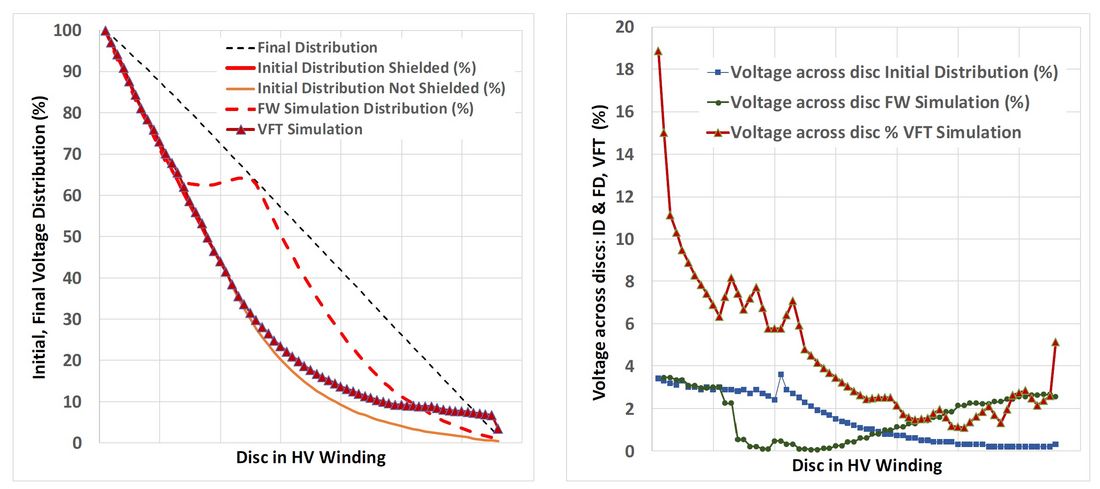
Figure 1 - Initial, Final Distribution and Voltage drop along the HV Winding of a 500 kV GSU transformer for 1.2/50μs BIL wave shape and VFT impulses (maximum of all 9 cases)
The two red lines represent the voltage distribution to ground from HV entrance to Neutral, red bold is the capacitive initial distribution, red dotted the result from real simulation. We can see that the ID works not so bad for the beginning part of the section with shielded conductor discs, but after some discs the difference increases between voltage drops derived from the ID and real simulation results. This is due to the fact, that simplified capacitive networks do not fit there anymore, because with the electrical distance to the HV terminal, the influence of inductive coupling increases, which finally makes the situation not really predictable in a precise way. We can see that the red dotted line is much closer to the FD than the ID. If we look to the other dotted lines, the blue dotted line indicates the voltage across the discs coming from ID, while the green dotted line represents the results for a real simulation.
To inform the reader: for the HV winding part at the terminal, a measure must be taken to realize a more linear voltage distribution– shielded wire technology is used in this case. We have a shielded and a non-shielded section in the HV winding. Looking at the voltage distribution we can now observe three areas: The first area is close to HV Terminal, here the ID fits well to the real voltage distribution, but when we look to the end of the shielded section, we see a big difference. Finally, when looking to the end of the winding, we see that the real transient simulation shows that the voltages increase versus ID. At the voltage inlet of the winding we observe 3.5% of BIL level while at the end we also observe 2.5%, not to oversee that in the middle of the winding the voltages are very low. It shows us that in general the voltage distribution is not predictable in a satisfactory way. At the end of the HV winding, the voltages across the discs are not close to zero – we need to rely on detailed simulations. The results are visualized for standard Full Wave shape, Figure 2. The behaviour for Chopped Wave is similar, but much more concentrated to the top region of the winding – and also limited due to the fact, that after chopping (typ. at 4μs) the voltage breaks down. Of course, in the design process, voltages are taken from models including capacitances, inductances and damping, which is industry standard since decades.
Figure 2 - Voltage distribution between LV and HV (middle entrance) for Full Wave (1.2/50μs)
Looking to VFT simulation we observe that the voltage distribution along the HV winding follows up to approximately 2/3 of the HV winding the simple capacitive ID. But when analysing the maximum voltage across the single discs it turns out, that the values are much higher as for FW simulation, due to the already indicated much higher non-linear voltage drop within and along the disc of the HV winding. Considering that for the numerical proof 1123 kV for VFT was used, while for FW 1550 kV is defined, we recognize that still for around half of the discs in the HV winding we get a much higher stresses than for standard FW simulation. Keeping also in mind that the duration time for VFT is much shorter. This shows out that a full turn wise model of the transformer is very important.
For VFT signals we observe a higher gradient over a larger part of the winding than for FW. Figure 3 shows the voltage distribution along the HV winding for VFT impulses (TR / TT = 10ns±50% / 165ns±60%) and standard Full Wave. The non-linear voltage distribution is also to be observed between the single turns of a disc winding.
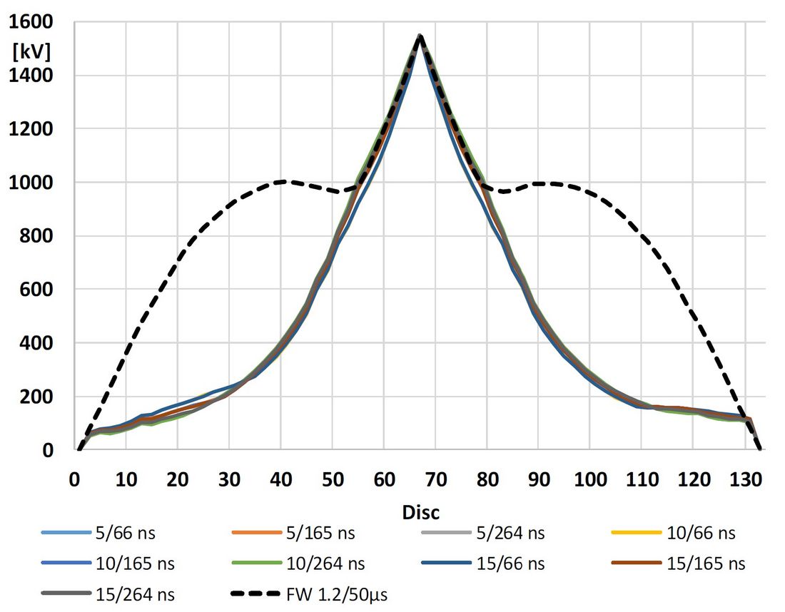
Figure 3 - Voltage distribution along HV, VFT impulses versus Full Wave
The difference between inner and outer part of the winding is due to radial shielded wire. While under FW we observe half of the Voltage across the disc pair between wire and shielded wire, under VFT we can observe more than 1.5 of that value, also in the not shielded section of the disc, Figure 4.
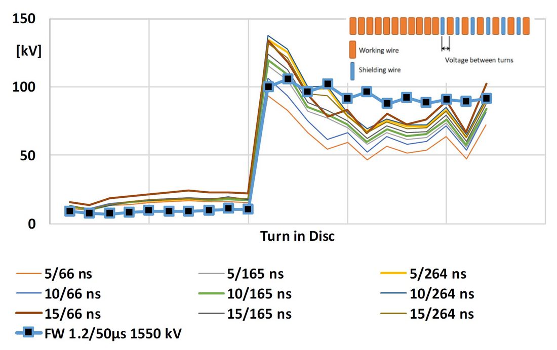
Figure 4 - Turn to turn voltage in the first disc at the HV terminal
Considering the effects of wave propagation we can also see that the maximum stress between discs does not occur any more at the inner or outer diameter of the winding but somewhere in the middle (depending on the chosen method for increasing the BIL withstand, i.e. radial interleaving or shielded wire technology). For a standard BIL simulation it is common practice to use a disc pair model – assuming a linear voltage distribution within the disc pair – figures 03 to 05 show clearly that this is not the case for VFT.
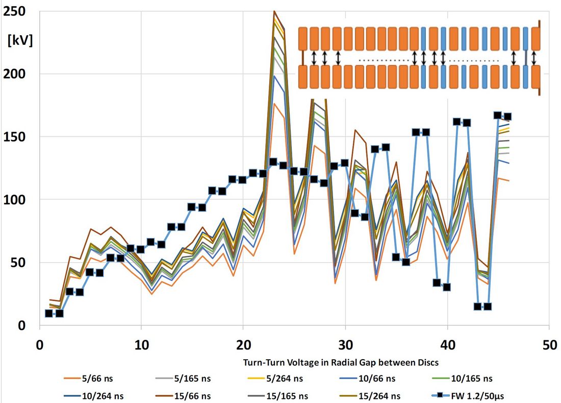
Figure 5 - Voltage distribution along the radial duct between the first two discs at the HV-entrance
The assumption of a linear voltage distribution is not valid any more for the required frequency range. It is important to point out that short time factors have to be applied to convert for these voltages into equivalent voltages.
4. Internal resonances
In [1, chap 4.1], a simplified procedure is described how to get a frequency dependent model of a transformer. This simplified approach is understandable, if there is not very much data about the internal setup of a transformer available. This situation is might be typical for the customers situation. A request for this simplified representation (figure 6) was also part of the customer requirement. Such models are valid only up to some kHz, because there are too few elements in the model. Consequently, the number of represented natural frequencies is low too.
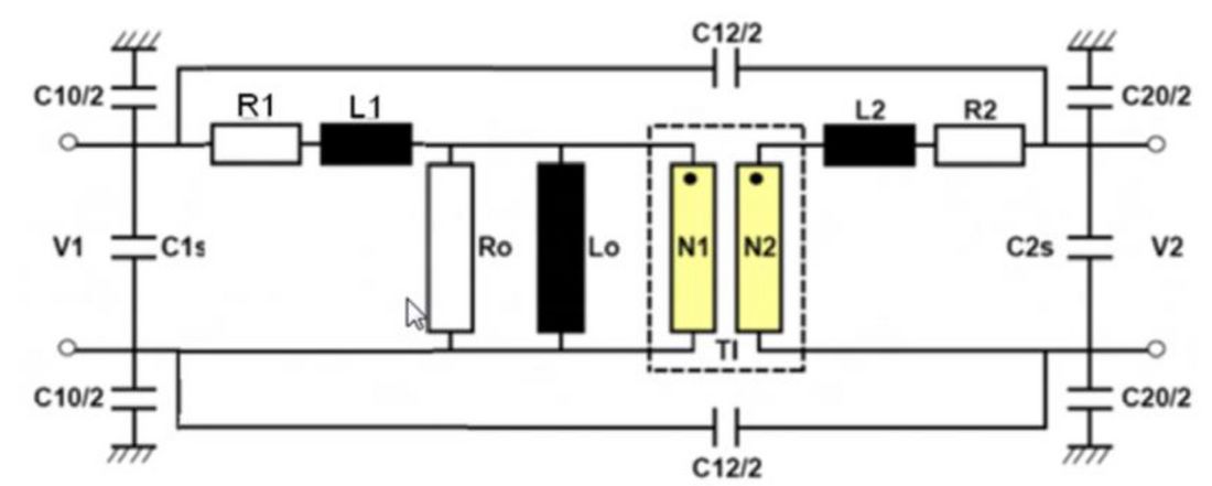
Figure 6 [1, Figure 4.1] - Combining a power frequency transformer T-model with an extern al capacitive network
As a manufacturer we use internal “white box models”, for which we can select different grades of detailing – typically hundreds of branches is standard. In Figure 7 the frequency response for 4 different models is given. The thin red line is according customer requirement – and in line with [1, chapter 4.1.1] – with a minimal number of branches. It is a representation with the minimum possible number of branches. It shows a significant difference for the model with a minimal number of branches compared to those with a higher number. Remarkable is, that a reduction to only one branch per winding is too extreme and accuracy is lost for transients. With at least some branches per winding, compared to the very detailed internal model we can see that the difference in the frequency response is very small.
It should be mentioned in general, there is no other option for manufacturers regarding modelling of transformers than the use of white box models. They can provide the internal voltages in a way that a proper insulation coordination is possible for the manufacturer. The mentioned Grey Box approach is not used in this case [1, chap. 4.5, comparison table]. For VFT studies it is also mandatory to use a much higher frequency solution than mentioned in [1, chap. 4.5]. The curve for the turn wise model in figure 7 demonstrates well, that for frequencies above 1 MHz the difference to simplified models increases. This is due a much more internal details, including also the bushing. This is also in line with [1] that conventional models fit to 500 to 800 kHz.
Anyway, the white box models can be represented in an equivalent RLC network and can be used in EMTP/ATP too. If it makes sense for the customer to proceed with a white box model resolution is an open question. The procedures and criteria for insulation coordination are intellectual property of each manufacturer. Besides large models also increase the customers simulation time in their application. As long as a terminal equivalent representation is sufficient, a reduced size models is recommended.
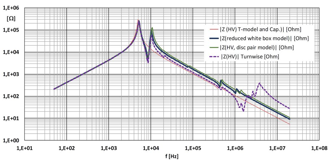
Figure 7 - Frequency response of different models in the range 50 Hz – 20 MHz. Impedance at HV
Terminal, Neutral and Low Voltage Terminals are grounded
From the reduced model the values for major resonance and anti-resonance frequencies can be derived. If the focus is on the terminal, we observe resonances, but we do not know in detail where they appear inside the transformer. Therefore, a detailed withstand evaluation (as usual within and between windings) was requested by the customer to proof the transformers withstand capability against signals with internal resonant frequencies. For the sinus at the input a damping factor of 0.8 was agreed.
A description can be found in [1, chap. 8.5.2], simulating a switching overvoltage (not VFTO) created by the power system. It must be mentioned that the first part of an impulse represents only ¼ of a full period while a continuous sinus represents more a quasi-periodic excitation. For example, with a SIL 250/2500μs the time to peak is 360μs → a similar frequency for a sinus is around 5kHz to 8 kHz, whatever we prefer to fit better into the rise of the wave (figure 8).
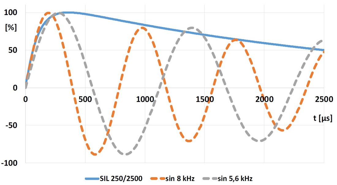
Figure 8 - SIL and “rise time fitted” damped sinus signals
According customers request we need to find out up to which voltage level a damped sinus applied at the HV terminal, is not harmful for the transformer – keeping in mind that ¼ of a sinus is fitting into the rise time of an impulse wave shape. It must be stated clearly that the standard task for the manufacturer is to provide a transformer capable to withstand specified single impulses.
For a high frequent periodic voltage input - even if damped - this is a challenge for the transformer. Results given in table 1. We can see, that for some periodic excitations a level from SIL is not allowable.
Therefore, the allowable voltage is given providing a safety margin of at least 1.25. This is a very worthful information for the customers, that for a damped sinus with 10.7 kHz and with an amplitude < 794 kV at the HV terminal the voltage are still no problem inside the winding (marg. ≥ 1.25) (table 01).
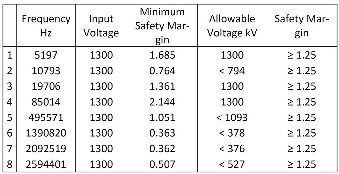
Table 1 - Allowable Voltages at HV Terminal (peak value)
Table 1 gives the minimum safety margin for each frequency with 1300 kV applied at the HV terminal. For a safety margin below the required 1.25 the input voltage is recalculated to the given value. It might be clear, that not only the HV winding would be the limiting factor for this kind of excitation. In figure 9 we can see, that for 10.7 kHz at the HV terminal it takes 2 ¼ periods to reach the maximum for the voltage between the first two discs in the HV winding, until the voltage decreases again.
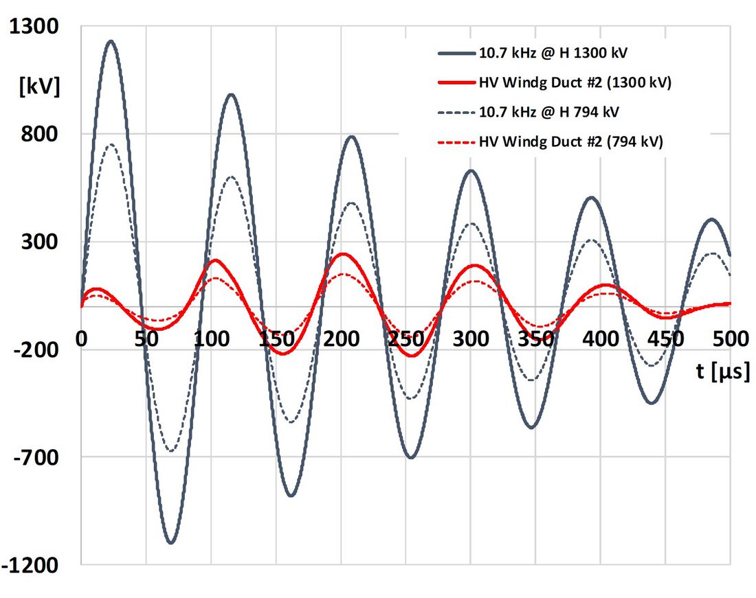
Figure 9 - Input 10793 Hz, voltage in radial duct number 2, after the HV terminal (between shielded wire ends)
Switching events are single pulse events – for this periodic excitation it takes 1¼ cycles of 10.7 kHz with 1300 kV at the HV terminal to exceed the local limit.
Limiting the allowable voltage to 794 kV at the HV (with damping 0.8) would not create any damage and keeping a margin of 1.25 (dotted lines in figure 09).
5. Withstand capability using customers signals
Transformers are often exposed to stresses which are not covered by the international standards. Therefore, it is a worthful information if signals from on-site measurements or from customer driven system studies are harmful for the transformer. Consequently, a proof of the withstand capability was done for energization, inductive opening and disconnection events. The signals were provided by the customer, the most critical was the disconnection event, plot given in figure 10.
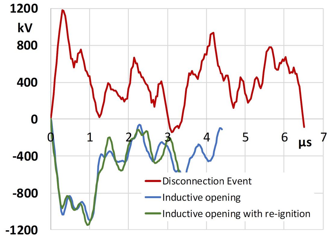
Figure 10 - Disconnection and inductive opening of Transformer HV. For the disconnection event a voltage of 1200 kV and a frequency range up to approx. 5 MHz needs to be considered
For the evaluation of the voltage stresses the Time Domain Severity Factor TDSF [1, chap 6.3.2] as well as the Frequency Domain Severity Factor FDSF [1, chap. 6.3] was done for all requested analysis. This is in full agreement with [1 chap. 6.3, TDSF]. For signals that are not covered by the standards it is helpful to calculate the Frequency Domain Severity Factor (FDSF). An explanation is given in [1 chap. 6.4.3].
is the envelope of the acceptance test frequency responses (SIL, FW, CW), figure 11.
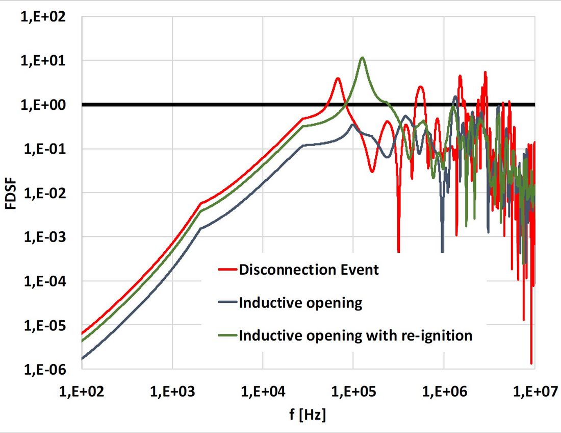
Figure 11 - Frequency Domain Severity Factor for customer signals. Xe(jw) is represented as a bold line (value 1.E+00)
Using the square of the frequency responses means that we are comparing energy involved in the transient with the energy involved in the standard test waves. However, if the FDSF is below 1.0 in all frequencies and the transients considered has a single dominant frequency, then it is highly expected that the transformer is protected against failures due to internal resonances. If the FDSF is above 1.0, the transient being analysed is not well represented by the standard wave tests.
Therefore, only an analysis with the white box models gives us reliable knowledge about the transformers withstand capability. Figure 11 is indicating well that inductive opening with re-ignition, and the disconnection event are not fully covered by the standards.
6. VFT test in manufacturers test lab with a SF6 chopping device
A final proof for the withstand capability was done by a special test by applying a SF6 chopping de-vice – creating a very high steepness during chopping. This was done according customer requirement.
An impulse with 900 kV peak, at a chopping time Tchopping = 1μs, and a steepness of ~300 ns could be reached during chopping, see Figure 12. The test sequence is given in table 2.
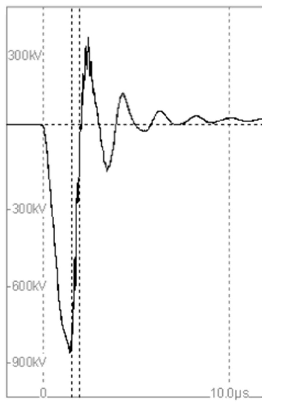
Figure 12 - VFT test impulse. Steepness 300 ns
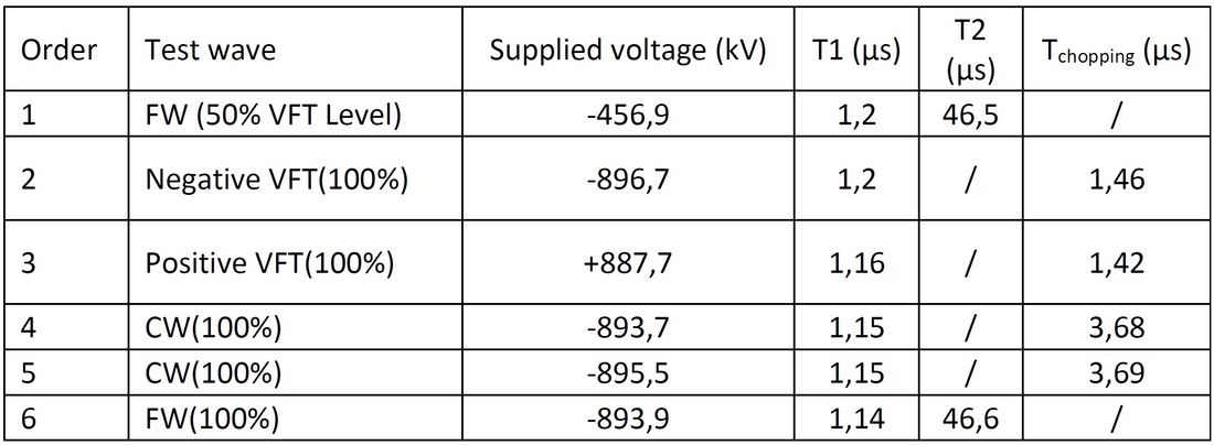
Table 2 - Test sequence for the 500 kV GSU (all phases tested)
Acceptance criteria: the cutting time of the VFT should be less than 2.6 μs. There is no break-down during the test, the tolerance of the testing voltage is limited to ±3%.
7. Conclusion about test and simulation
It was shown that a simplified transformer T-model does not even represent all resonance frequen-cies below 10 kHz, and therefore it is not a good basis for any simulation when frequencies around at least 10 kHz are important. Adding some more nodes in a white box model is sufficient for a terminal equivalent representation of the transformer’s impedance up to some hundred kHz, but not for VFT simulation. The reduced white box models were delivered to the customer and may be used in own system studies.
For signals, coming from on-site measurements as well as from customer system studies, the calcula-tion of the FDSF according CIGRE [1] gives insight whether this is covered by the Factory Assessment Test or not (as long the main character is of impulse wave shapes). As this is not fulfilled a numerical proof for the withstand capability was done by the manufacturer using internal white box models.
Due to the high frequencies in the customers signals as well as the VFT impulses it is essential to use models with a good frequency resolution above 1 MHz, which is in line with [1], pointing out, that conventional models fit only up to maximum 500 to 800 kHz (depending on the size of the trans-former). Consequently, for the withstand evaluation for customer driven signals and VFT impulses it was demonstrated that a turn wise model of the total transformer is essential to get a good knowledge about the voltage distribution under VFT stresses.
A practical proof of the transformers withstand capability was done using a special SF6 device to create a very early and steep chopping. It was demonstrated that the transformer was designed well to withstand all these impulses. Considering also that chopping started at 1.1 μs it proofs that the transformer withstands well “needle” impulses.
8. Comment about withstand capability for VFT stresses
Several literature has been published in which the breakdown behaviour of oil impregnated paper (OIP) with VFT-impulses was investigated. No work has been done with an original VFT-impulse.
The investigations have been done with different wave shapes: single short impulses [5], high fre-quency oscillating AC voltages [6], impulses like lighting impulse with a short front time (in same cas-es with tail times like the switching impulse)[7][8][9] and impulses like lighting impulse with a short front time and a oscillating frequency [7][10][11].
By comparing these different works, there are some discrepancies in term of the reported break-down strength of OIP material: some works indicate a higher electrical breakdown strength like [5][6], and other works like [7-11] indicate a lower electrical breakdown strength compared to the standard lightning impulse (1.2/50μs).
Based on internal criteria covering also the short time behaviour below 1μs and the fact that stresses under VFT are below some hundred ns, an adequate margin needs to be considered. It is well known for manufacturers that the withstand capability for impulses shorter than 1.2/50μs increases, but this behaviour does not continue to duration times around some few ns. With regard to the published literature it is necessary to point out that still some tests and investigations which cover more the real situation inside transformers under VFT stresses could be very helpful.
References
- CIGRE TB 577A (2014) Electrical Transient Interaction Between Transformers and the Power System, Part 1- Expertise, Joint Working Group A2/C4.39.
- CIGRE TB 577B (2014) Electrical Transient Interaction Between Transformers and the Power System, Part 2- Case Stud-ies, Joint Working Group A2/C4.39.
- S. Narimatsu, K. Yamaguchi, S. Nakano, S. Maruyama (1981) Interrupting Performance of Capacitive Current by Disconnecting Switch for Gas Insulated Switchgear (IEEE Transactions on Power Apparatus and Systems Vol. PAS-100, No. 6; June 1981).
- W. Boeck, R. Witzmann (1989) Critical GIS Configurations with Respect to VFT (Sixth International Symposium on High Voltage Engineering, New Orleans-LA USA, August 28 – September 1, 1989).
- Ikeda, M.; Fukumoto, S.; Takao, H.; Ohtsuka, S.; Haginomori, E.; Hikita, M. (2002) Breakdown Characteristics of Oil and Paper Insulation for a Very Fast Transient Voltage, Electri-cal Engineering in Japan, Vol. 141, No. 4, 2002, © 2002 Wiley Periodicals, Inc.
- Nakanishi, K.; Fujita, S.; Kurita, H.; Kishi, A.; Shibuya. Y. (1997) High Frequency Voltage Oscillation in Transformer Windings and Electrical Breakdown Proper-ties of Interturn Insulation Immersed in Oil at VFT Voltage, 1997 IEEE Annual Report-Conference on Electrical Insulation and Dielectric Phenomena, Minneapolis, October 19-22, 1997.
- Krithika, S.; Usa, S. (2013) Volt-Time Characteristics of OIP Under Non-Standard Impulses, CATCON2013, 978-4799-0083-1/13/$31.00©2013 IEEE, 2013.
- Vandermaar, A.J.; Wang, M.; Neilson, J.B.; Srivastava, K.D. (1994) The Electrical Breakdown Characteristics of Oil-Paper Insulation Under Steep Front Impulse Voltages, IEEE Transactions on Power Delivery, Vol. 9, No. 4, October 1994, 0885-8977/94/$04.00©1994 IEEE, 1994.
- Wang, M. (1991) The Electrical Breakdown Characteristics of Oil/Paper Insulation under Fast Front Voltages, Mas-ter-Thesis, University of British Columbia, 1991.
- Bavisha, T.; Usa, S. (2017) Impulse Breakdown Characteristics of Aged Oil Impregnated Paper, IEEE Transactions on Dielec-trics and Electrical Insulation, Vol. 24, No. 4, August 2017, DOI:10.1109/TDEI.2017.006456, IEEE 2017.
- Bavisha, T.; Aniruthaan, K.; Usa, S. (2017) Withstand Capability of Transformers under Very Fast Transients, 2017 3rd International Con-ference on Condition Assessment Techniques in Electrical Systems (CATCON), 978-1-5386-3138-6/17/$31.00©2017 IEEE, 2017.

- [1] CIGRE TB 577A (2014) Electrical Transient Interaction Between Transformers and the Power System, Part 1- Expertise, Joint Working Group A2/C4.39. // CIGRE TB 577B (2014) Electrical Transient Interaction Between Transformers and the Power System, Part 2- Case Studies, Joint Working Group A2/C4.39.
- [2] S. Narimatsu, K. Yamaguchi, S. Nakano, S. Maruyama (1981) Interrupting Performance of Capacitive Current by Disconnecting Switch for Gas Insulated Switchgear (IEEE Transactions on Power Apparatus and Systems Vol. PAS-100, No. 6; June 1981).