Converter Design for Multi-Terminal HVDC Systems with Partially-Selective DC-Circuit-Breaker-Based Protection
Authors
Marius KUHN, Lars OSTERKAMP, Willem LETERME - IAEW at RWTH Aachen University, Germany
Rodrigo ALVAREZ VALENZUELA, Zoi BLATSI, Sebastian SEMMLER - Siemens Energy Global GmbH & Co. KG
Patrick DÜLLMANN - IAEW at RWTH Aachen University, Germany & Siemens Energy Global GmbH & Co. KG

Summary
To ensure the stability of connected AC systems, selective DC-side protection systems comprising DC circuit breakers (DCCBs) and current-limiting inductors are foreseen for multi-terminal HVDC systems. To enable integration of half-bridge Modular Multilevel Converters in multi-terminal HVDC systems, it must be evaluated whether the protection system imposes additional requirements on the converter design. This paper assesses how DC-side protection system design influences converter responses during AC- and DC-side fault scenarios. Further, it proposes reduced test systems to analyse the impact of DC-side protection on converter performance and design. The investigated scenarios indicate that the DCCB speed is decisive for the ability of the future multi-terminal HVDC converter to continue operation after a fault, and even in that case, more submodules would be necessary to fulfil the same requirements. The required number of submodules varies significantly based on the protection system design, with fast DCCB-based schemes requiring the least adaptations.
Keywords
DCCB, HVDC, HVDC protection, MMC, multi-terminal1. Introduction
HVDC transmission systems are a key technology to enable large-scale integration of offshore wind, efficient transmission of large amounts of power over long distances and interconnection of asynchronous grids [1]. Currently, the vast majority of HVDC systems are realised as point-to-point (PtP) systems, each of which is provided by a single vendor [2]. Within these HVDC systems, Modular Multilevel Converters (MMCs) based on half-bridge submodules (SMs) are the most prominent converter technology due to their high efficiency and modularity [3]. Clearing of DC-side faults in current half-bridge-based PtP systems is realised by blocking the converter SMs and clearing the fault via AC circuit breakers (ACCBs) in the converter stations. This causes a complete shutdown of the HVDC link – or at least the affected pole in case of bipolar HVDC systems – and a power loss of up to its full transmission capacity [1].
To combine several of the aforementioned use cases and advantages of HVDC systems, the realisation of multi-terminal HVDC (MT-HVDC) hubs is envisioned for the near future [4], [5]. This development poses a major challenge, as a temporary shutdown of the entire MT-HVDC system after a DC-side fault could endanger the stability of the connected AC system(s). Therefore, MT-HVDC systems comprising MMCs without inherent fault blocking capabilities require dedicated DC-side protection. Such protection typically relies on DC circuit breakers (DCCBs) in series with inductors, which separate faulted parts of the system while maintaining the healthy part of the system in operation. Thereby, the maximum loss of power exchange with the AC system is limited.
Several studies have focused on the conceptual design of such DC protection systems and on deriving design requirements for the installed protection equipment [6], [7], [8], [9], [10]. This includes the specification of required DCCB performance and inductor ratings to achieve a desired DC fault ride-through (DC-FRT) behaviour of the converters on a system level. However, many existing studies rely on simplified converter models, which do not allow a detailed analysis of the converter-internal behaviour, e.g., the energy stored within the converter, during DC-side faults. Within [11], sensitivities between the converter electrical and control design and the protection design have been analysed. The obtained results highlighted the need to consider the impact of distinct converter responses when designing DC-side protection equipment, such as inductors and breakers. The inverse relationship, i.e., the impact of DC protection equipment on the design of the converter itself, has not been studied sufficiently within prior research and is therefore the focus of this paper. Besides the response during DC-side faults, an integration of large current-limiting inductors associated with DCCBs into an HVDC system will also affect the system behaviour in steady state as well as the dynamic behaviour during AC-side faults, which are important dimensioning scenarios for converters. Therefore, it is yet unclear whether established converter designs for PtP systems are transferable to MT-HVDC systems, in particular if DCCB-based protection schemes are applied. To answer this question, an assessment of the effect of DCCBs and inductors on the dynamic converter behaviour in the transient time domain for both AC-side and DC-side fault scenarios using detailed converter models is needed.
Based on the identified research gap, this paper aims to answer the following research questions:
- What is the impact of DC-side protection on the dynamic converter behaviour for AC-side and DC-side fault cases?
- Does the integration of converters into DCCB-protected MT-HVDC systems impose new requirements on the converter design compared to state-of-the-art designs for PtP links?
In the paper, reduced test systems are developed and implemented within electromagnetic transient (EMT) simulation software. These test systems are used to conduct parametric investigations on the impact of different MT-HVDC protection designs on dynamic converter performance under various fault scenarios. The dynamic performance is characterised by the transient behaviour of several converter-internal quantities. Based on a relative comparison of the converter performance and stresses to a benchmark scenario, which comprises an HVDC link with PtP converter designs, necessary design adaptations are identified to enable the integration of converters into MT-HVDC systems with various protection designs.
2. DC-Side Protection in MT-HVDC Systems
2.1. DC Protection Strategies
To minimise the impact of DC-side faults and ensure stability of adjacent AC grids, selective DC protection strategies have been developed for MT-HVDC systems [12]. These protection strategies rely on partitioning the MT-HVDC system into different protection zones. The separation between these protection zones is realised by DCCBs in series with current-limiting inductors. Based on the size of the protection zones, protection strategies can be classified as fully-selective (F-S) or partially-selective (P-S), as shown in Figure 1 for a four-terminal HVDC system with a DC switching station (DC-SS).
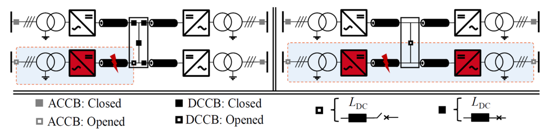
Figure 1 - DC Protection strategies in radial MT-HVDC systems (single-line diagram): fully-selective (left) and partially-selective (right), light blue area marking a protection zone
When a DC-side fault occurs, the system is divided into healthy and faulty protection zones via the DCCB(s). In the faulty protection zone, the converters enter the blocked state (indicated in red), and the fault is cleared via opening the ACCB(s) at the affected converter station(s). For the F-S protection setup, DCCBs are placed at each line end in the DC-SS. Hence, every line connecting a converter forms an individual protection zone. For the P-S protection setup, the system is split into two protection zones via a DCCB, thus providing a trade-off between the maximum power outage and the number of required DCCBs.
2.2. Converter DC-FRT Options
The behaviour of the converters in the healthy protection zone(s) can be characterised by their fault responses at the respective AC and DC point of connection (PoC). A classification of the PoC behaviour in three groups, based on the controllability of power exchange during a fault, is provided in [13]: Permanent Stop (PS) of power exchange, Temporary Stop (TS) of power exchange, i.e., without the system transitioning into an alarm state, and Continuous Operation (CO), i.e., no interruption of active and reactive power controllability. While the first two options would allow the converter to temporarily block, the converter must remain in unblocked operation for a CO requirement by this definition. Therefore, a DC-FRT of the healthy-zone converters in CO leads to the highest requirements on the DC protection. A temporary blocking of healthy zone converters, as proposed in [8], [14], [15], might relax the requirements on the DC protection design. However, it may endanger the AC system stability, especially with increasing duration of the blocking and de-blocking sequence. Therefore, such options are not investigated further within this paper, which focuses on the analysis of a DC-FRT in CO. In the definition of continuous operation used in this paper, i.e., retaining full control over active and reactive power, partially blocking a converter, e.g., a single arm, is also not allowed.
3. Converter Design in PtP and MT-HVDC Systems
3.1. Main Circuit Design
The PtP converter design process is well established and typically focused on a loss-minimal power transmission and compliance with AC grid codes [16], [17]. Crucial electrical design parameters of a half-bridge MMC (Figure 2) are:
- The modulation index M, i.e., the relation between the peak phase-to-ground AC voltage and the DC pole voltage,
- The inductances of arm and DC-side inductors (Larm and LDC,term),
- The number, nominal voltage and capacitance of the converter's SMs (NSM, VSM,ref, CSM), and
- The voltage and current ratings of the Insulated Gate Bipolar Transistors (IGBTs) (VSM,max, ISM,max)
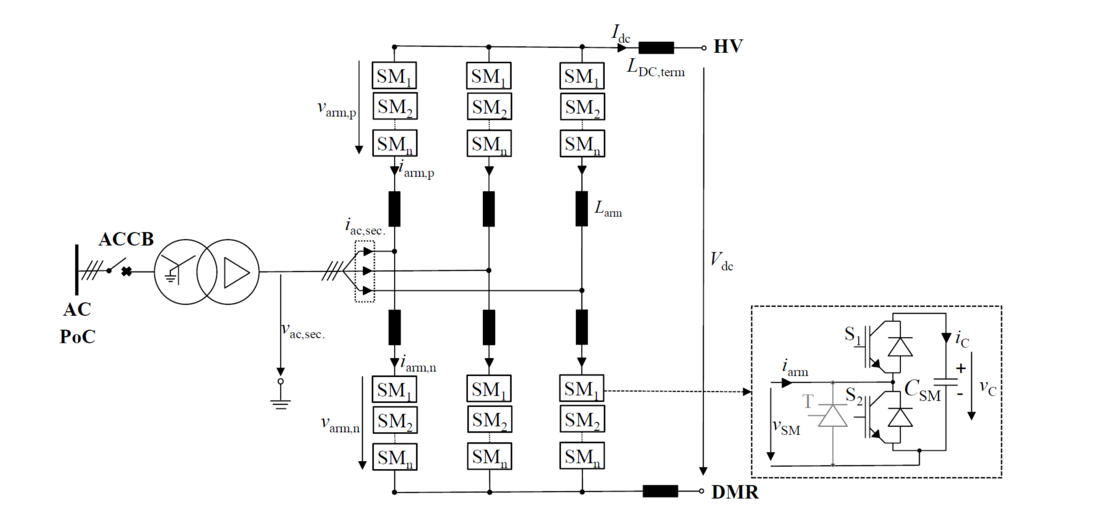
Figure 2 - Main circuit of half-bridge MMC connected to a bipolar HVDC system (P-pole)
Based on a given SM design with a fixed capacitance and nominal SM voltage, the minimum number of required SMs can be derived. The selected number of SMs must ensure that the energy stored within each converter arm, represented by the sum of all individual SM voltages, is sufficient to provide the arm voltage requested by the control during normal operation and dynamic events. This requirement can be derived by applying Kirchhoff's Voltage Law to the voltage loop comprising the AC-side voltage, DC-side voltage and arm voltage of the equivalent MMC circuit in Figure 2:
(1)
By inserting the negative peak values of the AC-side converter voltage 𝑣̂ac,sec, the voltage drop over the arm inductor Δ𝑣̂arm and the minimum DC voltage 𝑉DC, min to prevent overmodulation (cf. [18] for calculation), the minimum SM sum voltage can be derived. According to [19], [20], the maximum voltage drop over the arm inductor, neglecting resistive losses, is approximated as:
(2)
Here, 𝐿T denotes the transformer inductance and Pr and Qr represent the active and reactive power rating, respectively.
3.2. Converter-Internal Protection and Dynamic Converter Behaviour in PtP Systems
To protect the SMs in the event of faults, SM overvoltage and overcurrent protection are deployed. When the converter-internal protection thresholds are exceeded, the converter SMs are blocked [3]. In the blocked state, the current flows only through the antiparallel diodes and – if applicable – through protective thyristors. After the SMs are blocked, the fault current is interrupted by opening the converters' ACCBs. In existing PtP links, this fault-clearing process is applied for DC-side faults and converter-internal faults. For these fault types, the overcurrent protection typically acts the fastest [12].
In contrast, for AC-side faults of limited duration, the converter must preserve controllability and support the grid by injecting reactive current. This functional behaviour, referred to as AC fault-ride-through (AC-FRT) capability, is specified in existing AC grid codes [17]. Therefore, temporary AC-side faults should not trigger converter-internal protection functions. For AC-side faults, the SM overvoltage protection is highly critical [3].
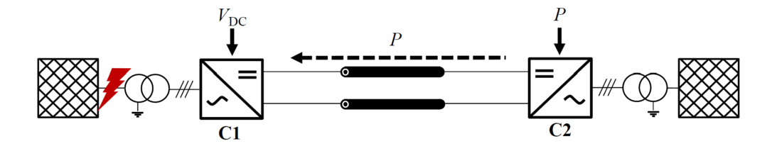
Figure 3 - Dimensioning AC-FRT scenario
This can be explained via the operational scenario shown in Figure 3, where power is transmitted from C2 to C1 and a fault occurs at C1, which is operating in inverter mode (responsible for DC voltage control). For a worst-case residual AC voltage of 0 kV, no active power can be transferred to the AC system connected to C1. As a consequence, the HVDC cable and the SMs of C1 charge and increase in voltage until C2's active power setpoint is reduced. Hence, operation in inverter mode at full rated power transfer must be considered as a worst-case scenario for analysing the dynamic converter performance in response to AC-side faults, with regard to overloading the converters' SM voltages.
3.3. Additional Converter Design Considerations for MT-HVDC Systems
Within MT-HVDC systems, compliance with DC-FRT requirements for healthy-zone converters, i.e., separated from the fault via a DCCB, must be ensured. In this paper, the basic criterion for a successful DC-FRT in CO, required for all healthy-zone converters, is to ensure that no submodules enter the blocked state due to converter internal protection. Th converter's DC-FRT is directly connected to the DC protection design, as well as to the converter design itself. This dependency can be expressed via the blocking time delay ΔtBLK, which specifies the time between the arrival of the travelling wave caused by a DC-side fault and converter blocking due to overcurrent protection [8]. As a prerequisite for a successful DC-FRT in CO, the total fault clearance time tclear, consisting of the fault detection time tdet and the DCCB opening time tDCCB, must be smaller than ΔtBLK. An analytical estimation of the blocking time delay is provided in [11]. This estimation could be used to provide first indications on the requirements for converter design for a given DC protection design. However, the analytical approximation loses accuracy if protection designs with higher ΔtBLK are considered and is derived for extreme cases of control reactions to DC voltage sags. Therefore, an EMT-based study is proposed for this paper.
Furthermore, the remaining energy of healthy-zone converters must be considered during DC-side faults. As DC-side faults cause a discharge of the converter, the fulfilment of the minimum SM sum voltage requirement specified in (1) needs special consideration in MT-HVDC systems in such fault scenarios.
As no operation of DCCBs as a fault-clearing device is intended for AC-side fault scenarios, the potential impact of the DC protection system on the dynamic system behaviour for such fault types is limited to the effect of the DCCB’s series inductance. To illustrate this effect, the AC-FRT scenario introduced in Figure 3 can be considered again. As explained in Section 3.2, the converter operating in rectifier mode must reduce its active power set point, and thus the DC current flowing through the line, as fast as possible to avoid critical charging of the DC cable and the SMs of the inverter station. If an additional DC-side inductance were present within the system, this decrease in the DC current would cause a release of the energy stored within the inductor’s magnetic field. The released magnetic energy will be converted into electrical energy, causing additional charging of the capacitances within the system. Therefore, an increase in the maximum SM voltages of the MMC during AC-side faults can be expected with increasing DCCB inductance.
To conclude, the converter design for selectively protected MT-HVDC systems must take the following additional aspects into consideration, which might cause different requirements compared to the state-of-the-art for PtP systems:
- For DC-side faults, converters in healthy protection zones must fulfil the respective DC-FRT requirements and do not block due to arm overcurrent (within this paper, CO of all healthy zone converters is assumed).
- The SM sum voltage of converters in healthy protection zones must be kept sufficiently high during DC-side faults.
- An increase of SM overvoltage with increasing inductance is expected during AC-side faults and must be kept below the protective limit to fulfil the AC-FRT requirements.
Figure 4 summarises the relevant converter-internal quantities for the investigations performed in this paper, alongside their corresponding protection thresholds marked in red (example values chosen for visualisation).
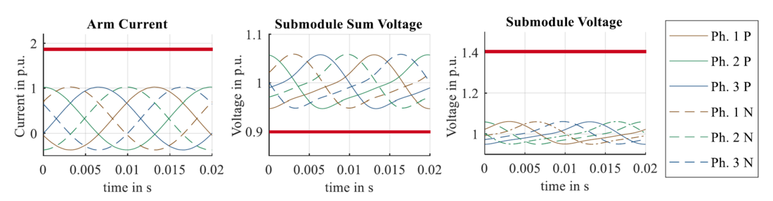
Figure 4 - Relevant converter-internal quantities for the analysis of the dynamic performance
4. Development of Reduced Test Systems
To approach the problem whilst simultaneously reducing complexity, reduced parametrizable test systems are proposed in this paper. As the first planned MT-HVDC systems in Europe will be realised as multi-terminal hubs in a radial structure, connecting the converters via a single DC-SS (cf. Figure 1), this topology is applied for the derivation of the test systems [21]. The core idea is to observe only the transmission between two converters and treat the rest of the MT-HVDC system as a disturbance. To identify this subsection, a case-by-case distinction based on the fault type under investigation (AC-side fault vs. DC-side fault), the DC protection strategy (F-S vs P-S) and the load flow scenario is conducted. As P-S protection systems are considered a promising option for the first MT-HVDC hubs [22], the analysis within this paper focuses on this protection strategy. However, the methodology to derive the reduced test systems is transferable to F-S protection systems.
4.1. Reduced Test Systems for AC-Side Faults
For the investigation of AC-side faults, the DCCB inductance is the relevant parameter of interest. Thus, the reduced test systems can be reduced to a PtP link with an additional equivalent inductor located in the DC system. The value of the inductance depends on the considered load flow. In Figure 5 (a), the derivation of the test systems for AC-side faults from an example radial four-terminal HVDC system is depicted. Within such a topology, specific load flow scenarios can be considered similar to a PtP connection between the two converters under study. The equivalent system, therefore, depends on the operational scenario. For a load flow scenario between C2 and C4 or C1 and C4, the equivalent PtP link comprises one DCCB inductance (Fig. 5 a).
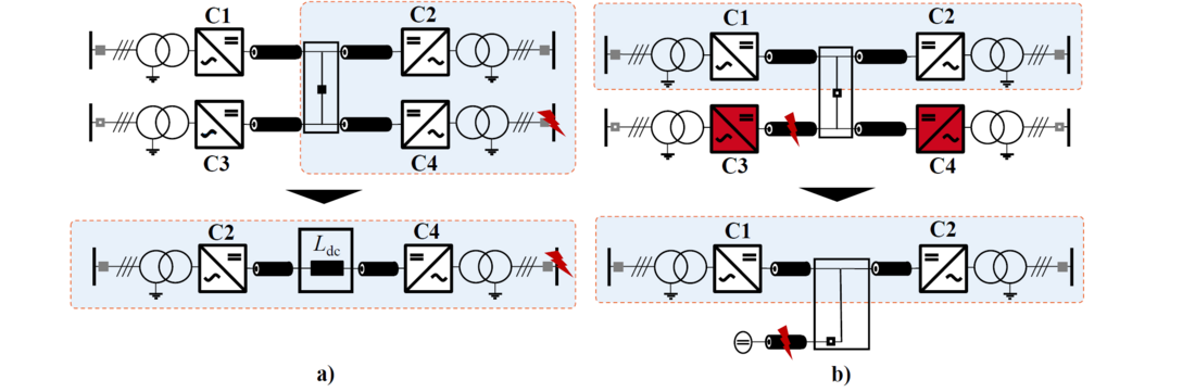
Figure 5 - Reduced test systems (single-line diagram): a) AC-side faults, b) DC-side faults
If a load flow between C1 and C2 or C3 and C4 were considered, the equivalent PtP link would comprise no additional inductor. However, as this conceptual scenario would be identical to a PtP reference case, it is not considered further. To account for different possible locations of the DC-SS, the line lengths in the equivalent setup are kept variable.
4.2. Reduced Test Systems for DC-Side Faults
To analyse the dynamic performance of healthy zone converters under DC-side faults, the equivalent test system must comprise a model of the healthy zone, a model of the DC-SS and a model of the faulty zone. Similar to the previous section, the healthy zone is modelled as a PtP link. In contrast to the setup for AC-side faults, the DC-SS model must not only include inductances, but also the DCCB itself. To account for different protection designs, a parametrizable DC-SS model is proposed.
As the detailed behaviour of converters within faulty protection zones is out of scope of this study, the faulty zone model is reduced accordingly. It consists of a DC voltage source connected to the healthy zone at the DC-SS via an additional cable, which enables a modelling of various fault locations and different pre-fault load flows across the DCCB. Figure 5 b) outlines the test systems for DC-side faults in a P-S protection system. Analogously to the setup for AC-side faults, the line lengths are kept variable. Different load flow scenarios can be evaluated by adapting the voltage setpoint of the DC source relative to the converters’ DC-side voltages. These test systems form the basis for an evaluation of the relevant converter properties identified in Section 2 for a variety of topologies, protection designs and fault types, while simultaneously reducing the computational effort, as only the relevant subsections of the MT-HVDC system are modelled in detail.
5. Component-Level Modelling
To conduct an EMT-based study, the developed test systems are implemented within EMT-type software for the framework of a bipolar HVDC system with dedicated metallic return (DMR). In this section, the modelling of the relevant components and their parametrisation is introduced. The MMCs are modelled using type-4 detailed equivalent circuit models (cf. [23]), which include a calculation of individual SM voltages. For the MMC control, an energy-based cascaded vector control structure based on [24] is applied, which includes a feed-forward (FF) of the measured DC voltage within the DC current control loop. During DC-side faults, this type of control tries to preserve the energy within the converter. It was identified within [11] that not only the electrical converter design but also the control design influences the DC-FRT behaviour. Hence, it should be noted that applying a different control structure may influence the expected results. While the case studies presented in this paper focus on the applied FF-type control architecture, as classified in [11], the developed methodology could be easily applied to various control designs by integrating different generic or vendor-specific control models. Cross-linked polyethylene cables are considered as the transmission technology for all lines, and modelled as frequency-dependent phase models. AC grids are represented by Thévenin equivalents with a fixed short circuit ratio (SCR) of 20 and an X/R ratio of 10. For DCCB modelling, the technology-independent, generic model proposed in [25] is used, which has been proven suitable for DC protection studies [26]. Within this model, the DCCB is represented as an ideal switch with a fixed opening-time delay in parallel to a surge arrester, modelling the transient interruption voltage generated in the energy absorption path. In series with this parallel path, a residual current switch is included to permanently isolate the faulted section. The fault detection and localisation are modelled in a simplified way: If an undervoltage relay detects a DC voltage below 0.85 p.u. at the DCCB terminal adjacent to the faulted protection zone, a tripping signal is sent to the DCCB after a fixed fault detection delay of 0.5 ms, which is a conservative estimation of the time a single-ended protection relay would need to selectively identify the fault. The system-level ratings and characteristic parameters of the cable model are specified in Table I.
| Symbol | Parameter | Rating |
| S | Rated power (per pole) | 1022 MVA |
| P | Rated active power (per pole) | 1000 MW |
| Vac,prim | Rated AC voltage (primary side) | 400 kV (RMS, L-L) |
| VDC | Rated DC voltage | ±525 kV |
| RDMR | DMR grounding resistance | 0.5 mΩ |
| Acore | Conductor cross-section | 2500mm² |
| R‘ | Length-related cable resistance | 7.2 mΩ/km |
| C‘ | Length-related cable capacitance | 0.217 µF/km |
| L‘ | Length-related cable inductance | 0.128 mH/km |
| VSM,ref. | Rated SM voltage | 1.485 … 3.6 kV |
| CSM | SM capacitance | 6…9 mF |
| Larm | Arm inductors | 27.1… 70 mH |
| Vac,sec | Rated AC voltage (secondary side) | 290…330 kV |
| VSM,max. | SM overvoltage protection threshold | 1.42VSM,ref |
| ISM,max. | SM overcurrent protection threshold | 1.83…2.1IDC,nom |
| VSM,sum,min. | Minimum arm sum voltage | 0.89 p.u. |
| LDC | DCCB series inductance | 10 mH…400 mH |
| tDCCB | DCCB opening time | 0.1 ms…8 ms |
| tdet | Fault detection delay | 0.5 ms |
For the electrical converter design, possible ranges for the main circuit parameters, derived from the system-level ratings and general PtP converter design considerations (cf. [19], [27]), are presented. For the case studies conducted in this paper, one arbitrary design within these parameter design ranges is chosen as a reference for demonstration purposes. To keep the results vendor-neutral and ensure the framework can be transferred if a different reference converter design is chosen, the converter’s dynamic performance is evaluated on a per-unit basis with respect to the thresholds specified in Table I. The thresholds for the SM overvoltage, relative to the nominal SM voltage, and SM overcurrent, relative to the DC current in normal operation, are selected based on typical ratings of commercially available SMs [11], [16]. The SM sum voltage threshold is calculated according to (1) and evaluated relative to the nominal sum voltage.

6. Impact of DC Protection on Dynamic Converter Performance
6.1. AC-Side Faults
6.1.1. Case Study
Within this case study, the dynamic converter performance is assessed for three-phase-to-ground and two-phase AC-side faults under various protection designs. Based on a pre-investigation in a reference PtP system, these fault types were identified as the worst-case symmetrical and asymmetrical AC-side fault types with regard to occurring SM voltages during the fault. All faults are applied at the AC PoC of the inverter station, operating at full power transmission pre-fault according to the worst-case scenario identified in Section 3.2. Converter C1 is in DC-voltage control mode, and C2 controls the active power. The faults are applied for a duration of 150 ms with a fault resistance of Rf,AC = 0.5 Ω. To capture worst-case conditions, the fault inception time is varied in 2.5 ms steps across one 20 ms power-frequency period. This accounts for the sinusoidal nature of the converter-internal quantities. To investigate the impact of the DCCB series inductance LDC, identified as the relevant protection parameter for AC-side faults, it is varied in a range between 0 mH and 400 mH. The range of inductance values is extracted from relevant literature [7], [8], [9], [10]. An overview of the test setup for this case study is provided in Figure 6.

Figure 6 - Test setup for AC-side fault case studies (single line diagram)
The DC-SS (i.e., the inductor) is located directly at C1 and connected to C2 via a 400 km cable. For all investigated scenarios, the SM voltages at the inverter station are evaluated to investigate potential converter overloading. To evaluate the natural behaviour of the SM voltages, the SM overvoltage protection is deactivated for all simulations.
6.1.2. Results
Higher inductance LDC results in increased charging of the SMs at the inverter station for both the two-phase fault and the three-phase-to-ground fault (Figure 7). For all investigated values of LDC, the two-phase fault leads to the highest maximum SM voltage (cf. Figure 7, left). In the reference PtP scenario (LDC = 0 mH), the maximum SM voltage reaches 1.4 p.u., thus not triggering the SM overvoltage protection. An increase in inductance above 200 mH causes a violation of the SM overvoltage threshold of VSM,max = 1.42 p.u., and would therefore lead to SM blocking if the SM voltage protection function were active. For the highest investigated inductance value of 400 mH, the prospective maximum SM voltage reaches almost 1.46 p.u., corresponding to an increase of 4.3 % compared to the reference PtP scenario without additional DC-side inductance.
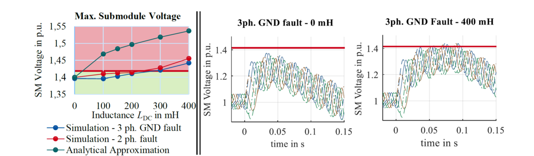
Figure 7 - Left: Maximum submodule voltages during symmetrical and asymmetrical AC-side faults for different inductance values; Right: Submodule voltages in the time domain
The extreme cases of 0 mH and 400 mH differ not only in maximum SM voltage but also in the time at which it occurs (Fig. 7, right). As a reduction of the active power injected into the DC system is required to achieve the desired AC-FRT behaviour (cf. Section 3.2), the dynamic converter behaviour for this scenario is strongly control-related. Therefore, the observations are in line with previous studies, which highlight the effect of large DC-side inductances on control dynamics, leading to slower dynamic response [28]. To account for the fact that the AC-FRT behaviour might differ if a different converter control were applied, the simulative investigations are complemented by an analytical approximation of the inductance’s effect on the AC-FRT behaviour. Based on the pre-fault DC current, the energy stored in the inductance’s magnetic field can be calculated as
(3)
Assuming a full reduction of active power transfer during the fault (IDC à 0), this magnetic energy would charge the DC cable and the SM capacitors. The distribution of the released energy between the cable and the SM capacitors depends not only on their respective capacitances but also on the converter control. Charging of the DC cable would result in an increase in the DC voltage, which should be limited to prevent component failures of cables and accessories [29]. Hence, a full transfer of the magnetic energy to the converter’s SMs is considered as a worst-case approximation. Assuming an equal distribution of the energy between all SM capacitors of the converter, the total energy transferred to the converter is calculated as
(4)
Since (3) and (4) must be equivalent according to the law of conservation of energy, the voltage increase per SM, Vsm,add, can be calculated as a function of the inductance LDC:
(5)
This approximated voltage increase, relative to the maximum SM voltage obtained from the simulation for LDC = 0 mH, is depicted by the green curve in Figure 7 (left). Since the analytical approach neglects the energy stored in the DC cable, it overestimates the increase in SM voltage compared with the EMT study. Nevertheless, it could be useful as a worst-case approximation, covering a range of possible control options.
6.2. DC-Side Faults
6.2.1. Case Study
For this case study, pole-to-ground faults at the external cable connected to the DC-SS are considered. Five different fault locations between 0 % and 100 % of the total cable length lext = 400 km are investigated, as the worst-case fault location may vary depending on the DCCB opening time due to travelling wave phenomena. The fault resistance is set to Rf,DC = 0.1 Ω and the fault inception time is varied in the same manner as for AC-side faults. As investigated in [30], rectification at full power is the worst-case operational condition in terms of the blocking time delay due to the DC offset of the arm currents. Therefore, full power transmission from C2 to C1 at rated power of 1 GW per pole is considered as a pre-fault load flow scenario for the case study. C1 operates in DC-voltage control mode, and C2 operates in active power control mode. The DC-SS is located directly at converter C2, operating in rectifier mode, while C1 is connected to the DC-SS via a cable with l12 = 400 km (cf. Figure 8). Within a pre-investigation, this was found to be the worst-case DC-SS location with respect to the maximum arm currents at the rectifier station. P-S protection strategies are investigated, with inductance values ranging between 10 mH and 400 mH. To represent a variety of potential DCCB technologies, ranging from fast power-electronic DCCBs to slower mechanical DCCBs, the DCCB’s opening time is varied in a range between tDCCB = 0.1 ms and tDCCB = 8 ms. An additional fault-detection delay tdet = 0.5 ms is assumed, irrespective of the DCCB technology under consideration. A two-step approach is used to assess the MMCs’ DC-FRT behaviour: First, the maximum arm currents in converter C2 are evaluated, identifying protection designs, i.e., combinations of LDC and tDCCB, which prevent blocking of healthy zone converters due to arm overcurrent. In a second step, the SM sum voltages of converter C2 are evaluated with respect to (1) for all protection designs which fulfil the first criterion.

Figure 8 - Test setup for DC-side fault case studies (single line diagram)
6.2.2. Results
To illustrate the different criteria which must be fulfilled to achieve the desired DC-FRT behaviour of converters in healthy protection zones, Figure 9 depicts the arm currents and SM sum voltages in the six arms of converter C2, operating in full rectification, for two example P-S protection designs in the time domain for the first 30 ms after fault inception. For the protection design shown on the left, comprising a DCCB with an opening time of 3 ms in series with a 200 mH inductance, the arm current protection threshold of 1.85 p.u., indicated in red, is exceeded and thus, the converter is blocked at t ≈ 7 ms. Once the converter is blocked, no current flows through the SM capacitors and the SM sum voltages thus remain at a constant level, reaching a minimum of 0.918 p.u. in the arm with the lowest residual SM voltage. By contrast, a protection design with an identical DCCB but a larger inductance of 250 mH sufficiently limits the arm currents to 1.74 p.u., such that the converter overcurrent protection is not triggered. However, the converter SMs therefore discharge further, and the SM sum voltage falls below the required minimum of 0.89 p.u., indicated by the red line, in two of the six arms. Both of these protection choices would therefore require adaptations of the reference converter design: the first due to current-related constraints, the second due to voltage-related constraints.
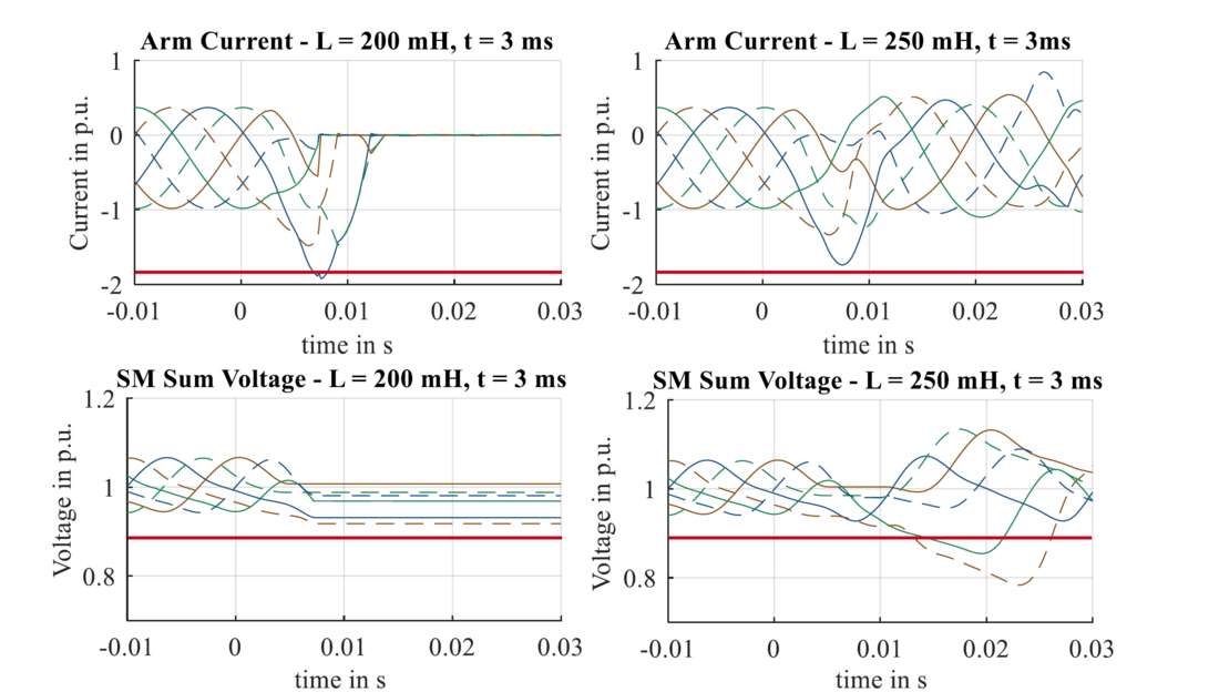
Figure 9 - Arm currents and SM sum voltages of healthy zone converter C2 for different protection designs in the time domain
In the following, the observations are generalised by sweeping through the defining protection parameters, namely inductance and DCCB opening time, as shown in Figure 10. For each protection design, the worst-case over all fault locations and fault inception times is depicted. A clear trend is apparent: DCCBs with a faster opening time require smaller inductances. If a fast DCCB with an opening time of 0.1 ms is deployed, a range of potential inductance values satisfies the current criterion indicated by the green-shaded area. For DCCBs with opening times of 1.5 ms and 3 ms, inductances of at least 100 mH and 250 mH are required, respectively. Notably, for the DCCB with an opening time of 8 ms, there are no inductance values which can sufficiently limit the current until the DCCB opening.
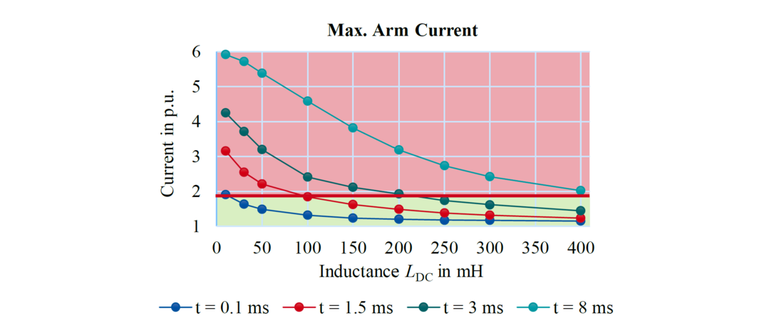
Figure 10 - Maximum arm currents for different protection designs
To ensure compliance of converters with such a protection design, the only viable option would be to increase the SM overcurrent protection threshold. This would require developing SMs with higher current ratings, which is not a trivial task. Thus, the advantages of a fast DCCB might enable the reuse of existing state-of-the-art submodules.
However, not only the current-related requirements, but also the voltage-related requirements must be fulfilled. Therefore, an evaluation of the minimum sum voltages for those protection designs fulfilling the current-related requirement is provided in Figure 11.
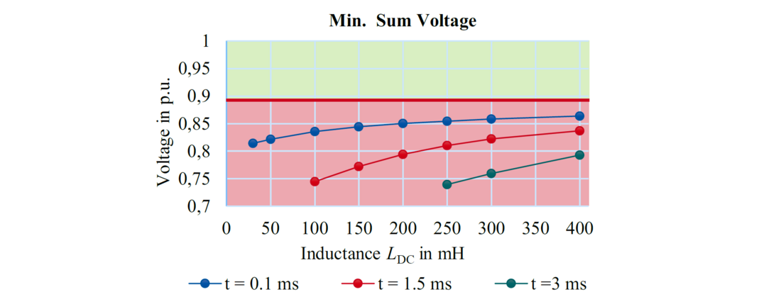
Figure 11 - Minimum sum voltages for different protection designs
The analysis reveals that the required voltage band to provide the required arm voltages (VSM,sum,min. ≥ 0.89 p.u., marked by the area highlighted in green) is violated for all investigated protection designs. A clear dependency of the minimum sum voltage on both the DCCB opening time and the inductance is observable. An increased SM discharge for lower inductance values can be observed, as lower inductances are accompanied by a higher rate of rise of the DC-side current. While this trend is noticeable for all investigated DCCB opening times, it becomes more severe as tDCCB increases. Furthermore, lower sum voltages are observed for higher DCCB opening times, as the relevant timeframe for SM discharge increases. The worst-case sum voltage discharge to a value of 0.74 p.u. occurs for a protection design comprising a DCCB with 3 ms opening time in combination with a 250 mH inductance. This observation indicates that the longer discharge period, determined by the DCCB speed, has a larger impact than the current-limiting effect of inductance.
A viable combination of LDC and tDCCB should fulfil all investigated voltage- and current-related criteria, i.e., be located in the green area in Figure 7, Figure 10 and Figure 11. As is evident, no DCCB configuration satisfies all three criteria. Therefore, converter redesign is in fact necessary.
6.3. Converter Design Adaptations
Based on the case studies, it can be concluded that an integration of converters with the given reference design - developed based on the requirements in PtP systems - into an MT-HVDC system is not compliant with the derived requirements for the investigated DC protection designs without further converter design adaptations. Depending on the protection design, one or multiple of the design criteria, derived from the AC-FRT and DC-FRT requirements, are not fulfilled. These unfulfilled design criteria are summarised in Table II. Here, the maximum SM voltage is related to AC-side faults (cf. Section 6.1), while the maximum arm current and minimum sum voltage are related to DC-side faults (cf. Section 6.2).
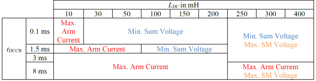
Table II - Unfulfilled design criteria for AC-side and DC-side faults
To assess options for design adaptations, a distinction is made between current- and voltage-related design constraints in the first step. The current-related constraints are related to converter blocking. As a consequence, they can be assessed through the analytical estimation of the blocking time delay [11], which depends on the following parameters: overcurrent capability K, AC-side voltage vac,sec and inductances Larm and LDC,term.An adaptation of these quantities may require significant changes to the converter design: increasing the overcurrent capability would require the development of new SMs; a reduction of vac,sec would increase steady-state losses; and increasing converter inductance would affect the dynamic behaviour of the control.
In terms of voltage-related design constraints, two different aspects need to be considered. To achieve the desired AC-FRT performance, individual SM voltages must be kept below the SM overvoltage protection threshold. On the other hand, the SM sum voltage in each arm must remain above the minimum to provide the required arm voltages. The simultaneous fulfilment of these requirements can be ensured by adapting the number of submodules per arm NSM and their respective nominal voltage VSM,ref. To comply with the AC-FRT requirements, the nominal voltage VSM,ref must be reduced such that the additional SM voltage rise caused by the DCCB’s series inductance LDC does not trigger the SM overvoltage protection. Therefore, NSM must be increased such that the average SM sum voltage in normal operation, equal to the product of NSM and VSM,ref remains constant.
To assess the necessary design adaptations in terms of additional submodules per arm, arising from the AC-FRT requirements, the results from Section 6.1 are reconsidered. For inductance values causing exceedance of the SM overvoltage protection threshold, i.e., LDC ≥ 200 mH (cf. Figure 7), an iterative adjustment of NSM and VSM,ref based on EMT-type studies is performed, ensuring that the protection limits are respected for the considered fault scenarios. Assuming the worst-case protection setup with an inductance of 400 mH, this design constraint would result in an increase of the number of SMs per arm of 5.4 % compared to the reference converter design. The required additional SMs and the resulting AC-FRT performance are depicted in Figure 12.
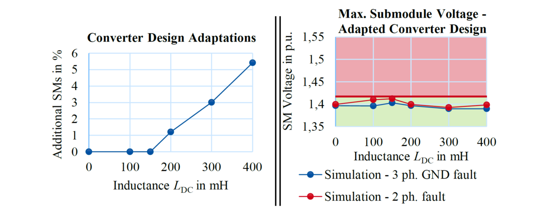
Figure 12 - AC-FRT performance with an increased number of submodules
To ensure a certain minimum sum voltage not only in normal operation but also during DC-FRT of healthy zone converters, the required number of SMs may increase further, depending on the protection design. To assess this, the minimum sum voltages depicted in Figure 11 are revisited. In a first approximation, the number of additional SMs required to comply with the sum voltage criterion can be calculated for each protection design by the ratio of the minimum required sum voltage of 0.89 p.u. to the minimum measured sum voltage:
(6)
For a protection design with a 3 ms DCCB and an inductance of 250 mH, such as the one shown in Section 6.2, this would result in an upscaling of Nsm,add,DC = 0.89 p.u./0.778 p.u. = 1.144, i.e., an increase of the number of SMs per arm of 14.4 %, solely attributed to the minimum sum voltage requirement. However, for some protection designs, both voltage-related constraints are violated when assuming the reference converter design. As for these protection designs, the voltage of each SM must be reduced to comply with the AC-FRT requirements, the resulting number of SM required to provide the minimum sum voltage during DC-side faults is increased even further, by a factor of
(7)
The converter design adaptations necessary to simultaneously comply with both voltage-related constraints for different protection designs are summarised and visualised in the design chart shown in Figure 13. Depicted are only those protection designs for which the prevention of converter blocking due to violation of current-related constraints is ensured. Notably, with reduced DCCB opening time, the admissible inductance range narrows and shifts toward higher values. The results obtained with the analytical approximation (7) are validated by an iterative adjustment of NSM and VSM,ref based on EMT-type studies, ensuring that the AC-FRT and DC-FRT requirements are fulfilled.
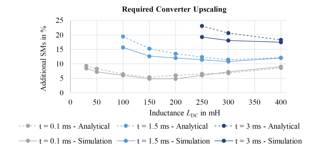
Figure 13 - Required converter upscaling to comply with AC-FRT and DC-FRT requirements
Especially for protection designs which necessitate a comparatively low upscaling, the analytical approximation allows an accurate estimation of the required additional SMs. With an increasing number of additional SMs, the analytical approach loses accuracy and tends to overestimate the required upscaling. While for all investigated protection designs an upscaling of at least 4.8 % additional SMs is required, the degree of upscaling strongly depends on the opening time and series inductance of the DCCBs. Protection designs with faster DCCBs result in lower upscaling, as the SM discharge during DC-side faults is limited by the DCCB’s fast response. In terms of the series inductance, two opposing effects overlap. The required upscaling resulting from AC-FRT requirements increases with increasing inductance. By contrast, the required upscaling due to DC-side fault scenarios increases for lower inductance values, especially when combined with slower DCCBs. Therefore, the inductance value leading to the highest overall upscaling requirements depends on the choice of DCCB technology. For the worst case across all considered protection designs (LDC = 250 mH and tDCCB = 3 ms), an increase of the number of SMs by 19.3 % would be required for the investigated system. Protection designs with a fast DCCB (tDCCB = 0.1 ms) and inductances between 150 mH and 200 mH require the least severe design adaptations.
6.4. Discussion
In the initial PtP converter design, the number of SMs is defined by functional performance requirements. To account for SM failures and maintain this functional performance over the converter’s lifetime, a number of additional redundant SMs may be installed in practice. The number of such redundant SMs is highly vendor- and project-specific. However, these redundant SMs are installed as a reliability margin rather than as a buffer during dynamic events. Therefore, any potential redundant SMs are not considered available to fulfil the new requirements in MT-HVDC systems identified in Figure 13.
The obtained results are based on a feed-forward-type control structure (cf. [11]) of the MMCs, which aims to keep the SM sum voltages constant during DC-side faults. Based on the investigations in [11], different control approaches are expected to result in a more pronounced SM discharge. As the SM discharge was found to be a primary driver of the necessary converter design adaptations, alternative converter control approaches may require more significant converter upscaling.
The results highlight the benefits of fast DC-side fault clearing for converter design. However, the practical implementation depends heavily on the availability and performance of the required switchgear. Currently, various DCCBs technologies are at a technology readiness level of 6 to 7 in Europe, according to [31]. While fast fault clearing has been shown to benefit converter design, it imposes strict requirements on the applicable DCCB technologies. A techno-economic assessment addressing the trade-offs between converter design and DCCB design is beyond the scope of this paper, but is recommended for future work.
7. Conclusion
Converters integrated into MT-HVDC systems with DCCB-based protection schemes require an adapted design compared to the reference design for PtP systems for all investigated DC-side protection designs. Depending on the specific protection design, these necessary design adaptations may result from violations of current- or voltage-related design requirements. These requirements stem from the arm current limits, submodule voltage limits and submodule sum voltage limits, which must be fulfilled during AC- and DC-side faults. To fulfil the current-related requirements, the DCCB opening time and its series inductance must be coordinated to prevent converter blocking. Fulfilment of the voltage-related design criteria can be ensured by increasing the number of SMs in the converter compared to the reference design for PtP systems.
The equivalent test systems proposed in this work enable a systematic assessment of the impact of DC protection on converter design for both AC-side and DC-side fault scenarios and various protection designs. For AC-side faults, protection designs with larger inductances were found to cause an increased submodule charging due to the additional energy stored in the inductance’s magnetic field. As a result, converter upscaling is required to prevent SM overvoltage and achieve the desired AC fault-ride-through performance. For DC-side faults, the required SM sum voltage band was violated for all investigated protection designs. The worst-case SM discharge – causing the most significant design adaptations – occurred for protection designs with slower DCCBs in combination with smaller inductances. From a combined evaluation of both AC-side and DC-side faults, it can be concluded that protection designs utilising faster DCCBs require the least amount of upscaling. The optimal inductance value needed to minimise converter upscaling varies depending on the DCCB opening time. Among all investigated protection designs that prevent blocking of healthy zone converters under DC-side faults, the required upscaling to meet all considered design requirements ranged from 4.8% to 19.3%. In conclusion, the findings of this paper emphasise the importance of considering the influence of DC protection system design during the converter design process for MT-HVDC systems.
References
- D. van Hertem, O. Gomis-Bellmunt, and J. Liang, HVDC Grids: For Offshore and Supergrid of the Future: John Wiley & Sons, 2016.
- ENTSO-E, "ENTSO-E Position on Offshore Development - Interoperability," 2021. [Online].
- K. Sharifabadi, L. Harnefors, H.-P. Nee, S. Norrga, and R. Teodorescu, Design, Control and Application of Modular Multilevel Converters for HVDC Transmission Systems: John Wiley & Sons, Ltd, 2016.
- North Sea Wind Power Hub Programme, "Towards the first hub-and-spoke project," 2021. [Online].
- ENTSO-E, "European Offshore Network Transmission Infrastructure Needs," 2024. [Online].
- I. Jahn, G. Chaffey, N. Svensson, and S. Norrga, "A holistic method for optimal design of HVDC grid protection," Electric Power Systems Research, vol. 196, p. 107234, 2021, doi: 10.1016/j.epsr.2021.107234.
- PROMOTioN, "Deliverable D4.2 - Broad comparison of fault clearing strategies for DC grids," 2017. [Online].
- M. Abedrabbo, W. Leterme, and D. van Hertem, "Systematic Approach to HVDC Circuit Breaker Sizing,"IEEE Transactions on Power Delivery, vol. 35, no. 1, pp. 288–300, 2020, doi: 10.1109/TPWRD.2019.2922253.
- P. Torwelle, K. Shinoda, P. Verrax, A. Zama, and A. Bertinato, NSWPH MT HVDC Functional Requirements:: Step-by-step guide on functional requirements and parameter ranges definition for hvdc building blocks. [Online].
- P. Tünnerhoff, C. Brantl, D. Ergin, F. Schettler, A. Schön, and D. Döring, "Impact of the DC circuit breaker design on selective fault detection and clearing methods in multi-terminal HVDC systems," in 15th IET International Conference on AC and DC Power Transmission (ACDC 2019), 2019, pp. 1–6.
- P. Düllmann, C. Brantl, C. Klein, and A. Moser, "Interdependencies in HVDC grid protection: Impact of converter parameters and controls on DC fault-ride-through capabilities and protection system design," IET Generation, Transmission & Distribution, vol. 17, no. 10, pp. 2356–2375, 2023, doi: 10.1049/gtd2.12812.
- CIGRE TB 739, JWG B4/B5.59, "Protection and local control of hvdc-grids" Paris, 2018
- HVDC Grid Systems and connected Converter Stations – Guideline and Parameter Lists for Functional Specifications: Part 1: Guidelines, CLC/TS 50654-1, CENELEC, 2022.
- M. Zaja and D. Jovcic, "Coordination of mechanical DCCBs and temporary blocking of half bridge MMC," in 15th IET International Conference on AC and DC Power Transmission (ACDC 2019), 2019, pp. 1–6.
- K. Shinoda, P. Torwelle, and P. Verrax, "InterOPERA D2.1: Functional Functional requirements for multi-vendor multi-terminal HVDC grids," 2024.
- R. Alvarez, M. Wahle, H. Gambach, and J. Dorn, "Optimum semiconductor voltage level for MMC submodules in HVDC applications," in 2016 18th European Conference on Power Electronics and Applications (EPE’16 ECCE Europe), 2016, pp. 1–9.
- Technical requirements for grid connection of high voltage direct current systems and direct current connected power park modules, VDE Verband der Elektrotechnik, Elektronik, Informationstechnik e.V., 2019.
- EPRI, "Expandable & Compatible HVDC Grid Design," 2024. [Online].
- PROMOTioN, "Deliverable D2.1 - Grid topology and model specification," 2016.
- P. D. Judge, G. Chaffey, M. M. C. Merlin, P. R. Clemow, and T. C. Green, "Dimensioning and Modulation Index Selection for the Hybrid Modular Multilevel Converter," IEEE Transactions on Power Electronics, vol. 33, no. 5, pp. 3837–3851, 2018, doi: 10.1109/TPEL.2017.2719103.
- TenneT TSO GmbH, Multiterminal-Hubs. [Online].
- V. Tackenberg, J. Welsch, and D. Stenzel, "InterOpera D3.1: Demonstrator Definition & System Design Studies," 2024.
- CIGRE TB 604 - WG B4.57, "Guide for the development of models for hvdc converters in a hvdc grid," Paris, 2014.
- P. Ruffing, "HVDC Grid Protection Based on Fault Blocking Converters," PhD Thesis, RWTH Aachen University, Aachen, Germany, 2020.
- M. Zaja, D. Jovcic, L. Kunjumuhammed, K. Tahata, T. Inagaki, and S. Nee, "Generic and simplified HV DC circuit breaker models for grid-level studies," in 2020 IEEE Power & Energy Society General Meeting (PESGM), 2020, pp. 1–5.
- CIGRE TB 873 - JWG B4/A3.80, "Design, test, and application of hvdc circuit breakers," Paris, 2022.
- D. Jovcic, High Voltage Direct Current Transmission: Converters, Systems and DC Grids: John Wiley & Sons, Ltd, 2019.
- W. Wang, M. Barnes, O. Marjanovic, and O. Cwikowski, "Impact of DC Breaker Systems on Multiterminal VSC-HVDC Stability," IEEE Transactions on Power Delivery, vol. 31, no. 2, pp. 769–779, 2016, doi: 10.1109/TPWRD.2015.2409132.
- CIGRE TB 657 - WG B4.56, "Guidelines for the preparation of "connection agreements" or "Grid Codes" for multi-terminal schemes and DC Grids," Paris, 2016.
- M. Abedrabbo, W. Leterme, and D. van Hertem, Impact of Operational Parameters on HVDC Circuit Breaker Requirements: CIGRE International Council on Large Electric Systems, CIGRE Science & Engineering.
- D. Hart, C. Foote, A. Mouhaidali, S. Rangasamy, A. Bertinato, and B. Marshall, "DC Circuit Breaker Feasibility Study -Protection System Design," Session 2024 Papers & Proceedings, 2024. [Online].