Methodology to define the arm inductance range in a Modular Multilevel Converter station for HVDC applications based on steady-state and DC pole-to-pole fault
Authors
J. SAU-BASSOLS, F. MOREL, K. VERSHININ - SuperGrid Institute, France

Summary
The arm inductance in modular multilevel converters (MMC) for high voltage direct current (HVDC) applications has a relevant impact in the performance of the converter in steady-state and during faults. This paper proposes the methodology to define a range of arm inductance values for a given MMC-HVDC station with fixed AC and DC voltage. The minimum value of arm inductance comes from protecting IGBTs, diodes and bypass thyristors in the submodules during a DC fault, while the maximum value comes from ensuring the steady-state PQ provision (ability to modulate the AC waveform with the DC voltage). A simplified MMC model is developed to calculate the converter fault currents. The sensitivity analysis shows that the constraints that define the minimum value of arm inductance depend on the case study, the most relevant being the IGBT turn-off capability, the maximum surge current of the diodes and the l²t of the bypass thyristors.
Keywords
arm inductance, DC fault, half-bridge, HVDC, modular multilevel converter1. Introduction
High voltage direct current (HVDC) based on voltage sourced converters (VSC) is seen as a key technology to facilitate the massive integration of renewable energy sources [1]. The preferred industrial solution to convert from high voltage alternating current (HVAC) to HVDC is the modular multilevel converter (MMC). This topology is based on the series-connection of submodules that allows the modulation of a stepped waveform to be very close to a sinusoidal waveform. It provides a modular and scalable solution with a very low harmonic content and low losses [2].
Among the different elements of the MMC, the inductance value of the arm inductors plays a relevant role in the converter operation. During DC fault conditions, it limits the di/dt of the fault current, meaning that the inductor can be designed to protect the semiconductors in the submodules [3]. Half-bridge submodules are the most common type of submodule employed in HVDC-MMCs. They have a low component count and lower conduction losses than full-bridge submodules, but they lack the ability to stop DC faults currents and the AC breaker is relied upon to stop the current during DC faults. A DC pole-to-pole fault is identified as the most severe external fault in terms of the fault current [4]. Consequently, several papers propose simplified models to calculate the fault currents of an MMC under a DC pole-to-pole short-circuit, which can provide the specifications of the arm inductor. Analytical expressions that describe the fault currents during different stages of the fault are derived in [5], [6], [7]. Other works employ simplified state-space representations of the MMC and calculate the fault currents numerically [8], [9], [10]. The aim of both approaches is to calculate the fault currents without needing to rely on time-consuming detailed simulations [11]. Usually, the peak current limit of the IGBTs in the submodules before their blocking is defined as one of the criteria to choose the arm inductor [12], [13]. Some works consider the peak current of the bypass thyristors [4] and the let-through energy l²t of the lower diode in the submodules [14], [7] to define the arm inductance value, taking into account also the stages after blocking the converter.
When direct modulation is used (without AC circulating suppressor), the arm inductance can be selected to avoid resonances with the submodules capacitances and to limit the peak of the circulating current [15], [16], [17]. However, in case of considering a circulating current suppressor [18], [19], the second harmonic current can be effectively limited, thus not affecting the arm inductance choice. This circulating current suppressor can be either based in software [19] or in hardware, for instance, by adding a capacitor between the two arm inductors [19], [20].
The combination of the arm inductance and leakage inductance of the transformer is referred to as phase inductance. This phase inductance affects the speed of the AC current control (using phase inductance values near 0.1 pu in most applications provides a simpler control [4]) and has an impact on limiting the negative-sequence currents [21]. It also serves as a filter to reduce the harmonic content introduced by the converter. In MMCs for HVDC applications, the high number of submodules lead to moderate filter requirements, thus, moderate values of phase inductance [4]. The value of inductance required for harmonic filtering is given in [7] and it corresponds to 0.125 pu for the considered case study. The phase inductance also creates an AC voltage drop when transmitting active and reactive power at PCC. For a defined AC voltage, if the inductance is too high, the given DC voltage may not be sufficient to modulate the required AC waveform to transmit the desired active and reactive power [4].
This work proposes a methodology to define a range of arm inductance values for a given MMC-HVDC station with an already defined AC and DC voltage, aggregating different criteria mentioned in various publications. The minimum value of arm inductance is obtained from the DC pole-to-pole fault criterion, which provides an inductance value that ensures the survival of the semiconductors in the submodules considering all the stages of the DC fault. The methodology checks that the maximum turn-off current of the IGBTs, maximum peak current of diodes and bypass thyristors, the I^2 t of diodes and bypass thyristors are below the maximum acceptable values for the semiconductors. The maximum value of arm inductance is obtained from ensuring that the voltage drop across the phase inductance does not affect the required PQ operating range of the converter. For that, a rectangular PQ characteristic curve is considered, in which the arm inductance requirement is defined for the operational point corresponding to the maximum active power and maximum capacitive reactive power at the same time. No over/under voltages or over/under frequencies are considered when calculating the arm inductance requirement. For the methodology presented in this paper, the AC and DC voltage of the MMC station are already defined and given as inputs. The aim is to define a suitable range of arm inductance values for a given MMC station, but not providing an optimum design of it that would require to consider many more degrees of freedom.
The contribution of this paper is the methodology to define a valid range for the arm inductance that ensures both the survival of all the semiconductors in the submodules (IGBTs, diodes and bypass thyristors) during a DC fault and the nominal provision of PQ in steady state for a given MMC-HVDC station with fixed AC and DC voltages. Furthermore, the sensitivity analysis shows how the setting of certain MMC parameters (other inductances, time delays, thresholds, etc.) changes the stress on some semiconductors but not others, allowing to modify the arm inductance requirement. Additionally, the impact of the AC voltage when calculating the arm inductance requirement is also assessed.
In section 2, the two aforementioned criteria are explained in detail. Then, a state-space model of the MMC is derived to perform simulations in a fast way that is illustrated in section 3. The workflow of the methodology, described in section 4, is applied to a case study based on a real MMC-HVDC link and the simplified model of the MMC is validated against a more detailed model in section 5. A range of inductance values complying with both criteria are given for the case study and then, different parameters are modified in the sensitivity analysis, in order to assess their effect on the required arm inductance values. Finally, the conclusions of the work are summarized in section 6.
2. Criteria to select the arm inductance
This work focuses on the following two criteria to select a value of arm inductance:
- C1: Limiting the fault current in a DC pole-to-pole fault to protect the semiconductors,
- C2: Ensuring that the voltage drop across the phase inductance does not affect the required PQ operating range of the converter.
2.1. C1: Limiting fault current to protect the semiconductors of the submodules
As mentioned before, this work considers an MMC with a DC pole-to-pole fault in a symmetric monopole. The same methodology and developed model could be used for studying the inductance requirements of a bipole under a pole-to-neutral fault without modelling the healthy pole and considering equivalent groundings. The study of other internal faults is considered as a future extension of this work. Some examples of internal faults could be a fault to ground between the valve of submodules and the arm inductor, a valve short-circuit, an internal short-circuit between arms, a fault to ground between the transformer and the valve of submodules, etc.
Since the submodules are half-bridge, the MMC has no capability to stop the fault current and the submodules must be blocked to protect the semiconductors. After the blocking, the AC grid feeds the fault and the lower diodes of the submodules inevitably conduct. After some cycles the fault current is finally interrupted by the AC breaker. However, during the duration of the fault, the semiconductors are subject to high currents depending on the fault stage. To protect them from the fault current after the blocking, the manufacturers have proposed two solutions: using diodes with a high surge current capability (approach used by Hitachi Energy [3]) or adding a bypass thyristor in parallel with the diodes to divert the current (approach used by GE and Siemens [3]). This work considers the latter (see Fig. 1), though the models can be easily modified to also implement the first one.
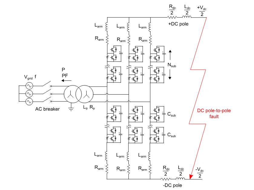
Figure 1 - Scheme of an MMC under a DC pole-to-pole fault
The DC pole-to-pole fault is divided into three stages, which imply different constraints for the diverse types of semiconductors in the submodules. The fault stages are presented below with the corresponding figures, illustrating the concerned semiconductors in each case and deriving five different subcriteria leading to a minimum requirement of the value of arm inductance.
- Stage 1: Just after the fault, before blocking the MMC
- Stage 2: After blocking the MMC, AC breaker closed
- Stage 3: After opening the AC breaker
2.1.1. Stage 1: Just after the fault, before blocking the MMC
During the instants after the fault, the arm and DC currents rise while some submodules are inserted (capacitors discharge) and others are bypassed (see Fig. 2(a)). The detection of the fault by the converter control is not instantaneous nor the order to block the submodules, it can take between tens and hundreds of microseconds.
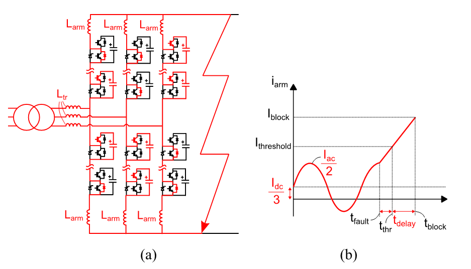
Figure 2 - DC fault stage 1. (a) Scheme of the MMC with inserted and bypassed submodules. (b) Blocking strategy based on a current threshold
The arm and DC currents rise with a di/dt that depends mainly on the voltage of the submodules, fault impedance, arm inductance and DC inductance (if present). At this stage most of the contribution comes from the voltage in the inserted submodule capacitors and not from the AC grid [6].
It is assumed that the fault happens when one of the arm currents is at its peak value (see Fig. 2(b)). Future work should investigate the effect that the instant of the fault has considering different phase angles of the AC waveform. After reaching an arm current threshold that indicates the presence of a fault (Ithreshold), a signal to block all the IGBTs in the submodules is sent (see Fig. 2(b)). A time delay between the sending of the signal and the actual blocking of the IGBTs is assumed. It can account for the sensor delay, the communication system delay to receive the sensor data, the protection system delay to issue block command, the communication delay to receive the block command by the submodule and the delay in gate driver of the submodule. The triggering of the bypass thyristors is assumed to occur at the same time as the IGBTs are blocked. The IGBTs in the inserted submodules must be able to turn-off the current at the moment of the blocking (Iblock). The same current circulates through the lower diode of the bypassed submodules, meaning that Iblock must also be lower than the maximum surge current of the diodes IFSM. This leads to two subcriteria:
- C1.1. Select Larm to ensure that
- C1.4. Select Larm to ensure that
where, is the maximum current that can be turned-off by the IGBT and IFSM is the maximum surge current of the diode. id corresponds to the current through the diode. It can be noticed that in C1.4, the value Iblock (value of current at the moment of the blocking) is replaced by id to have a more generic criterion that can be applied to other stages. It keeps the same constraint as using Iblock in Stage 1, since the highest value of id in Stage 1 corresponds to Iblock.
It must be noticed that this work considered this approach with the Ithreshold, tdelay, , IFSM to set a general criterion before the blocking of the IGBTs. Ithreshold is given as a parameter to assess its effect in the arm inductance requirement, this work does not aim at providing an optimum value for this parameter.
Additionally, other approaches such as limiting the maximum di/dt of the arm current can also be equivalent and can even be combined with the methodology presented in this paper.
2.1.2. Stage 2: After blocking the MMC, AC breaker closed
After the submodules are blocked, the submodule capacitors no longer feed the fault. The MMC acts similarly to a diode rectifier (with inductances in the arms) and the AC grid feeds the fault since the AC breaker is still closed (see Fig. 3(a)). Although the fault is not fed by the capacitors in stage 2, the peak of the arm current at this stage can be higher than in the stage 1 since the duration of stage 1 is significantly shorter than stage 2. The reason of this is that the blocking of the converter happens within tens or hundreds of microseconds, while the opening of the AC breaker takes tens or hundreds of milliseconds. Both the arm inductance and the leakage inductance of the transformer have an impact on limiting the peak of the fault current (higher values of inductance reduce the peak in both cases) [4]. During this stage, the bypass thyristors in parallel with the lower diodes are conducting, meaning that the fault current is shared between the two semiconductors according to their threshold voltage and on-state resistance. The current through the bypass thyristor (ithy) must be lower than the maximum surge current of the bypass thyristor (ITSM), leading to C1.2:
- C1.2. Select Larm to ensure that ithy ≤ ITSM
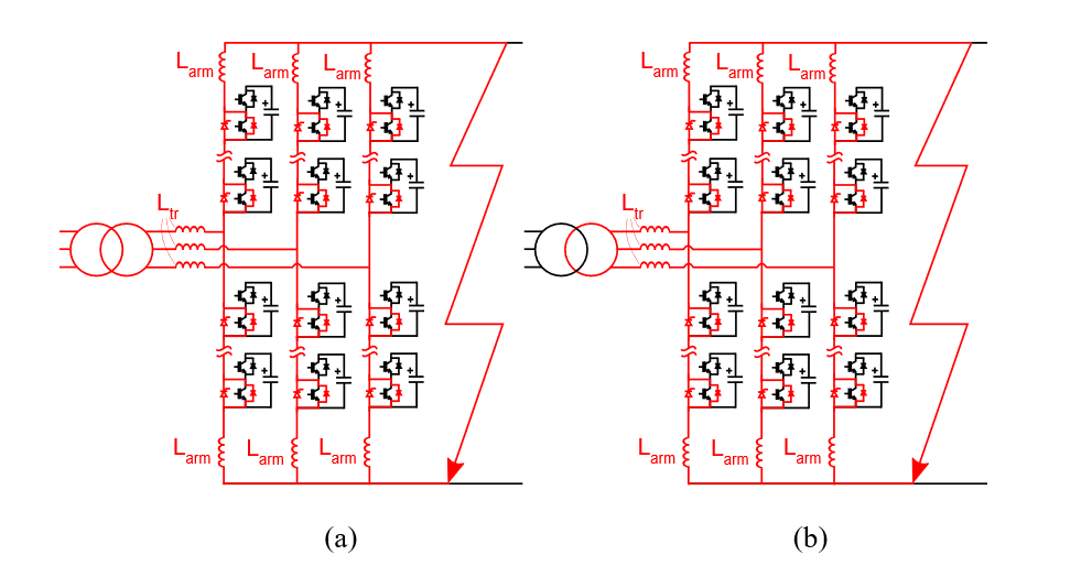
Figure 3 - Schemes of the blocked MMC during a DC fault. (a) Before opening the AC breaker (Stage 2). (b) After opening the AC breaker (Stage 3)
The peak current of the diode during this stage must also be lower than (IFSM), which is equivalent to C1.4, already introduced in Stage 1.
It is assumed that the semiconductors are the most vulnerable devices in terms of surge currents in the HVDC station. The other devices, such as AC breakers, transformers, etc. are assumed to be able to handle the fault currents.
2.1.3. Stage 3: After opening the AC breaker
After the opening of the AC breaker, the AC grid no longer feeds the DC fault (see Fig. 3(b)). The DC current and the arm currents decrease as a result of the discharge of the inductors in the system [13]. At this stage, the peak of the currents is lower than in the previous stage, but the diodes and thyristors may need to handle a current higher than the nominal for an extended period of time. Thus, the thermal limit of those devices must not be exceeded, which leads to two additional subcriteria:
- C1.3. Select Larm to ensure that
- C1.5. Select Larm to ensure that
The integral of the square of the current of the bypass thyristor (ithy) and the diode (id) must be calculated from the starting of the fault to the final instant where the fault current becomes 0 (from tini to tfin), since the thermal limit can be exceeded also in the previous stages.
2.1.4. Summary of C1 and its subcriteria
Based on the three fault stages, five different subcriteria have been identified to protect the semiconductors of the submodules. Some of these subcriteria have been introduced in the explanation of one of the stages of the fault, but they must be applied to other stages as well, as already mentioned in the text. The following list gathers the five subcriteria and the corresponding stages to which they have to be applied:
- C1.1. Select Larm to ensure that
(Stage 1)
- C1.2. Select Larm to ensure that
(Stage 2)
- C1.3. Select Larm to ensure that
(Stage 2, stage 3)
- C1.4. Select Larm to ensure that id ≤ IFSM (Stage 1, stage 2)
- C1.5. Select Larm to ensure that
(Stage 1, stage 2, stage 3)
It must be noticed that this work assumes that the semiconductors of the MMC are already defined when choosing the value of arm inductance. If this was not the case, and one of the subcriteria was not met (for example C1.2), instead of increasing the arm inductance value, an alternative could be to choose a bypass thyristor with a higher ITSM.
2.2. C2: Ensuring the voltage drop across the phase inductance does not affect the required PQ operating range of the converter
As mentioned before, this work considers that the AC and DC voltage of the MMC station are already defined and given as inputs. In practise, the AC voltage that the MMC sees can be adapted thanks to the transformer turns ratio (providing an additional degree of freedom for the design of the MMC station).
When exchanging power between the MMC and the PCC of the AC grid, the inductances in between (mainly arm inductance and leakage inductance of the transformer) cause an AC voltage drop. Fig. 4 shows the vector diagram of the simplified MMC operation based on two voltage sources and an inductance extracted from [4]. is the peak AC voltage generated by the MMC submodules,
represents the peak ac phase-to-ground voltage measured at the station terminals (the point of common coupling, PCC), referred to the transformer secondary winding (MMC side) and
represents the peak voltage drop across the phase inductance. The phase inductance Lphase is expressed in (1), as a function of the arm inductance and the leakage inductance of the transformer (Ltr).
(1)
is limited by the DC voltage of the MMC (Vdc). When using half-bridge submodules, the maximum voltage that can be modulated is Vdc/2. However, if considering third harmonic or zero sequence voltage modulation, the maximum voltage becomes 1.15Vdc/2 [22]. Since the voltage drop across the phase inductance is proportional to its inductance value Lphase, a high Lphase can lead to a high
that exceeds the modulation capability of the MMC. Then, the desired PQ provision cannot be guaranteed. The aim of this C2 is to provide the maximum value of arm inductance that ensures the PQ provision (upper limit), taking into account that the lower the value of arm inductance, the better, since the required voltage to be generated by the MMC becomes lower.
The highest constraint happens when the MMC injects the maximum active power and maximum capacitive reactive power (leading power factor) at the same time, since needs to be higher than
. Knowing the maximum voltage that can be modulated by the MMC allows to calculate the maximum phase inductance to guarantee the required PQ range [4].

Figure 4 - Vector diagram of the simplified MMC operation extracted from [4]
The nominal peak current at the PCC can be expressed as (2).
(2)
where, S, P and PF are the nominal apparent power, nominal active power and power factor at the PCC, respectively.
The base impedance is then expressed in (3).
(3)
Then, (4) shows the phase impedance a function of the base impedance, in which the factor kx can be understood as the phase inductance in pu value.
(4)
Replacing (2) in (4) and rearranging leads to (5), which corresponds to the peak value of the voltage across the phase inductance .
(5)
From trigonometry, a relation can be established between the three voltages and the angle , which is:
(6)
Also, knowing that , the following relation can be obtained from Fig. 4:
(7)
Combining (6) and (7) and replacing by PF yields to:
(8)
The roots of the previous expression are:
(9)
(10)
By combining (5) and (7), and then replacing by PF, it is possible to obtain (11)
(11)
Then, by combining (11) and (10), it is possible to obtain an expression (12) that depends on kx, PF, and
, whose roots are (13) and (14).
(12)
(13)
(14)
Since the value of kx must be positive, only (13) is considered to give the pu value of phase inductance as a function of PF, and
. If replacing
for the maximum voltage that the submodules can generate, the maximum value of kx is obtained (
), which allows the calculation of the maximum phase inductance.
From (1), it is possible to deduce that the maximum phase impedance is given by the sum of half the maximum impedance of the arm inductance and the leakage impedance of the transformer (15).
(15)
where, f is the frequency of the AC grid.
Then, by rearranging (15), it is possible to calculate the maximum arm inductance, which is given in (16).
(16)
This leads to C2:
- C2. Select Larm to be lower than
3. Models of the modular multilevel converter
This work considers two models of the MMC with different levels of detail: Model 1 and Model 2, which are presented below.
3.1. Model 1
Model 1 considers a symmetric monopole HVDC link with two MMCs, which are based on an average model with capability to represent DC faults. This model is used as a benchmark to perform the validation of Model 2 and it is illustrated in Fig. 5. The HVDC link is grounded on the AC side of MMC 1 using star-point reactor, which is then connected to a transformer represented by a leakage impedance. The primary of the transformer is then connected to an AC breaker and to the AC grid. The DC pole-to-pole fault is assumed to happen at the terminals of MMC 1 after the DC impedance (Ldc and Rdc). This DC impedance can be used to represent a parasitic impedance, fault impedance or the impedance of a DC inductor. The cables are modelled using a wide band model from [23].
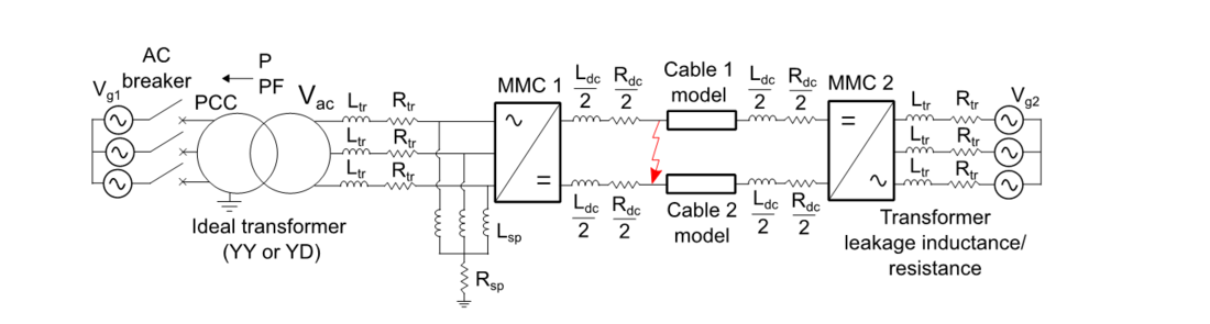
Figure 5 - Scheme of a symmetrical monopole HVDC link with two MMCs considered for the detailed model
The arms of the MMC are modelled as an equivalent controlled voltage source that represents the submodules (see Fig. 6). A controlled current source and an equivalent capacitor are used to model the charging and discharging of the submodules. An IGBT and a diode are included in parallel with the voltage source to model the blocked state (Blk=1 and m=1) [24] and a bypass thyristor is added in parallel with the lower diode as well.
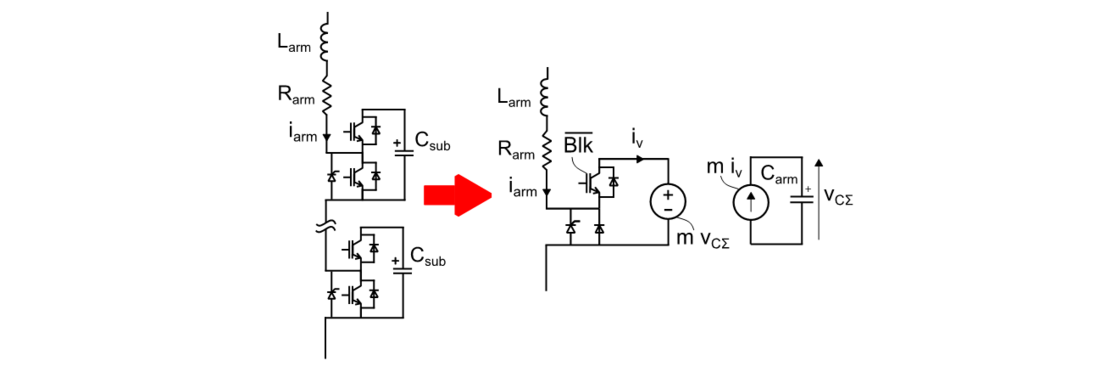
Figure 6 - Average model of one MMC arm with capability to represent the blocked state including the bypass thyristor
The control strategy of the HVDC link is as follows: MMC 1 regulates the DC voltage and the reactive power, while MMC 2 controls the active and reactive power. Both MMCs employ an energy-based control with the outer and inner loops described in [25].
The average model with blocked state MMC in Model 1 [24] is used as a benchmark for the validation of Model 2, since [24] shows that it provides accurate results for DC pole-to-pole faults and other situations, when compared with a 21-level detailed model MMC.
3.2. Model 2
Model 2 considers a simplified model of an MMC with a short-circuit in the DC side based on the work developed in [10]. It allows to represent the MMC before and after the blocking of the submodules and the opening of the AC breaker. The model of stage 1 before the blocking is illustrated in Fig. 7.
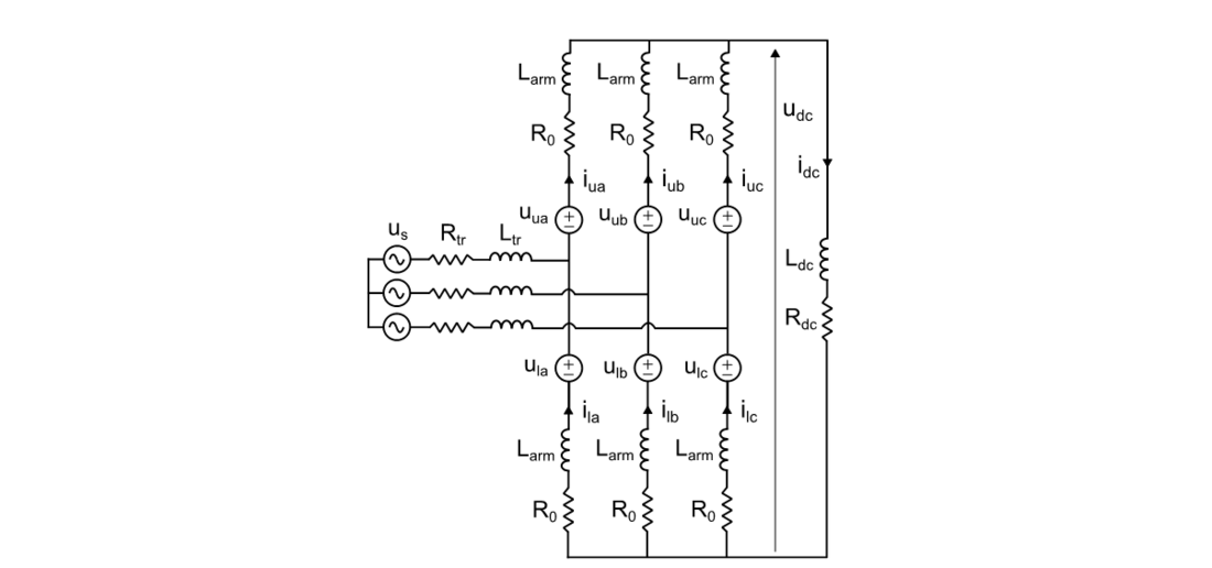
Figure 7 - Model 2 of the MMC before the blocking of the submodules (stage 1)
The model is implemented in a state-space representation given by the following equations:
(17)
where, Aconv, Lconv, Rconv are the matrixes of the state-space equation and iconv is the vector that contains the six arm currents of the MMC, as shown in (18). The details of the matrixes concerning the state-space model for each stage can be found in the Appendix.
(18)
The vector uconv contains the grid voltages, the arm voltages generated by the submodules and the threshold voltage of the thyristors in one arm, as expressed in (19).
(19)
The charging and discharging of the capacitors in the submodules are represented as a single capacitor model as in [10].
The model in Fig. 7, corresponding to stage 1, is dynamically modified depending on the fault stage of the simulation, leading to the models of Fig. 8 (for stage 2, after blocking) and Fig. 9 (for stage 3, after opening the AC breaker) in order to incorporate the different behaviours of the converter during the fault. The changes with respect the model of the previous stage are highlighted in green (see Fig. 8 for stage 2) and in blue (see Fig. 9 for stage 3) to facilitate the comprehension.
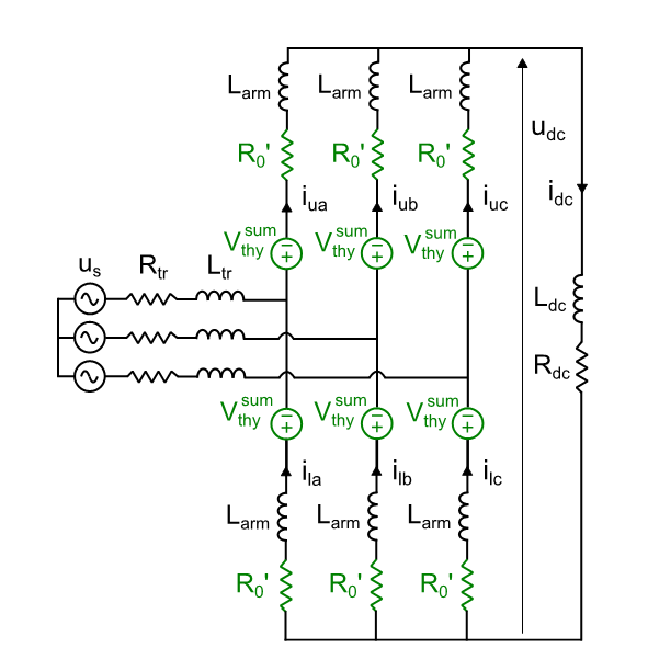
Figure 8 - Model 2 of the MMC after the blocking of the submodules, before opening the AC breaker (stage 2)
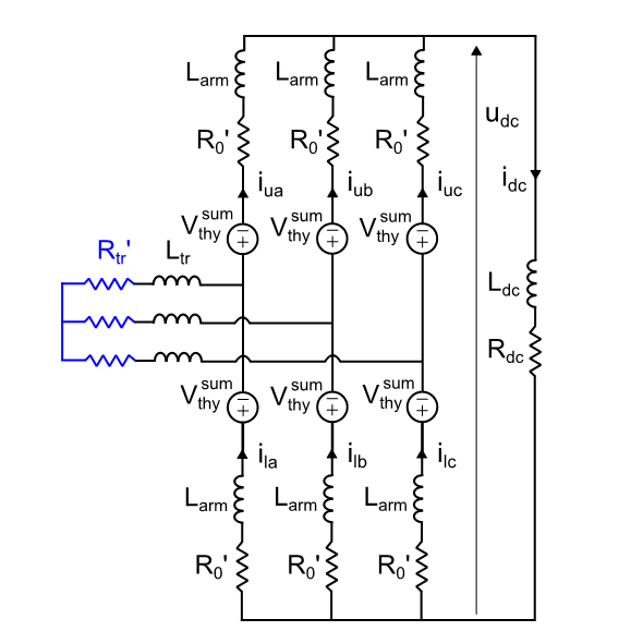
Figure 9 - Model 2 of the MMC after opening the AC breaker for each phase (stage 3)
The current-voltage characteristic of the semiconductor devices in the MMC (diodes, IGBTs and bypass thyristors) are modelled as a threshold voltage source and an on-state resistance.
3.2.1. Stage 1: before blocking the MMC
The arm voltage sources (uu and ul) in Fig. 7 represent the voltages generated by the stacks of submodules. us corresponds to the grid voltage referred at the secondary of the transformer (equivalent to Vac until the opening of the AC breaker in Stage 3). Rtr and Ltr represent the parasitic resistance and leakage inductance of the transformer. R0 gathers the parasitic resistance of the arm inductor and the on-state resistance of the IGBTs and diodes in the path of the current (the threshold voltage of both devices is neglected at this stage). Rdc and Ldc are the resistive and inductive part of the impedance in the DC side, which represent one or several of the following elements: impedance of the fault, parasitic impedance of the connections or the impedance of the DC inductor if present.
3.2.2. Stage 2: after blocking the MMC, AC breaker closed
In Fig. 8, the arm voltage sources (uu and ul) are removed. They are replaced by the sum of all the threshold voltages of the bypass thyristors conducting the current in the arm (). Although in reality, the current is shared between the diode and the bypass thyristor, the model is adjusted to assume that the current flows entirely through the bypass thyristors. The share of stress on each device is calculated offline at the later stage (see section 3.2.4.). In the model,
is defined as a variable resistance that assumes very high values when the current becomes negative (allowing to implement the unidirectional behaviour of diodes and thyristors). When the current is positive,
includes the parasitic resistance of the inductor and the on-state resistance of all the thyristors in the arm.
3.2.3. Stage 3: after opening the AC breaker
In Fig. 9, the grid voltages (us) and the transformer resistance (Rtr) that were presented in the model of stage 2 are dynamically modified to represent the behaviour of the AC breaker. When the current of one of the phases crosses 0, the corresponding grid voltage source is removed and the resistance Rtr' of that phase is increased up to a high value to model the opening of the AC breaker.
3.2.4. Offline calculation of the current sharing between bypass thyristors and diodes
As explained in Section 3.2.2, the model assumes, that during stage 2 and 3, the arm current entirely flows through the bypass thyristors to simplify the state-space model. Once the arm current is calculated following this hypothesis (iarm), the shared stress between bypass thyristors and diodes is computed according to the approach described in this section.
The model in Fig. 10 is used, where the bypass thyristor branch and the diode branch are represented. Both include a voltage source that represents the voltage threshold of the bypass thyristor (Vthy) and the voltage threshold of the diode (Vd). A resistance is also included in each branch modelling the on-state resistance of the bypass thyristor (Rthy) and the on-state resistance of the diode (Rd). An ideal diode in each branch to allow only positive currents is also included.

Figure 10 - Model to perform the offline calculation of the current sharing between bypass thyristors and diodes
The bypass thyristor is designed to have a very low voltage drop to ensure that most of the current flows through it, protecting this way the parallel diode. Both the threshold voltage and the on-state resistance of the bypass thyristor are lower than the ones of the diode (see Table II). Consequently, the arm current flows entirely through the bypass thyristor until its voltage drop reaches a value equal to the threshold voltage of the diode. When the arm current iarm reaches the threshold value given by (20), the diode branch starts to conduct.
(20)
When both branches are conducting, the current is shared so that it generates the same voltage drop in both devices. Therefore, knowing the parameters of both devices and the total arm current, the current circulating through the bypass thyristor (ithy) and the diode (id) can be estimated with (21) and (22).
(21)
(22)
4. Workflow for calculating the arm inductor range
As mentioned before, this work gives the methodology to define the arm inductance in a MMC station for HVDC applications based on steady-state and DC pole-to-pole fault. It is considered that the AC and DC voltage of the MMC station are already fixed and given as inputs. The aim is to define a suitable range of arm inductance values for a given MMC station, but not providing an optimum design of the MMC, which would require to consider many more degrees of freedom.
The flowchart of the proposed method to calculate acceptable range of arm inductance values of an MMC is shown in Fig. 11.
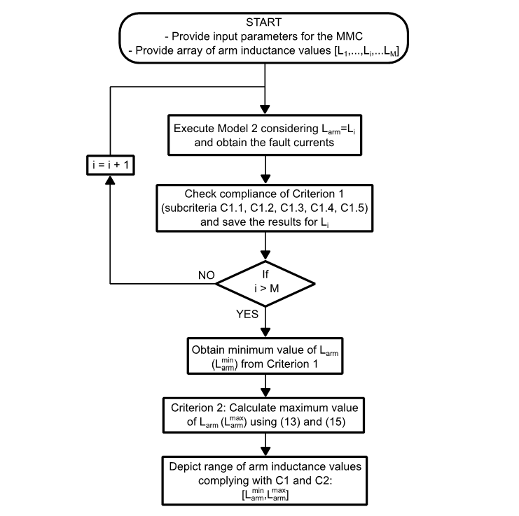
Figure 11 - Flowchart of the methodology to obtain the acceptable range of arm inductance values for an MMC
First, the parameters of the MMC and the system are defined. Along with them, an array of arm inductance values is also given as input. The subscript i is used to identify each value of arm inductance being tested and the subscript M identifies the last value of arm inductance to be tested. The methodology consists in executing Model 2 for each of the arm inductance values. The arm currents during the fault are obtained for each arm inductance value and the Criterion 1 is verified, including all the subcriteria, obtaining the minimum value of arm inductance that complies with Criterion 1. The maximum inductance values according to Criterion 2 are obtained from (13) and (16). With both a minimum and a maximum value of arm inductance, it is possible to define a range of inductances that comply at the same time with Criteria 1 and 2: .
If no additional criteria are considered, when choosing an arm inductance within the acceptable range, selecting the minimum value leads to a cheaper option, when looking only at the arm inductor. When designing a new HVDC project many more aspects have to be considered.
5. Case study and validation
A case study considering an MMC-HVDC link based on INELFE Spain-France interconnection [26] is used to show the results of the methodology. A validation of Model 2 is performed by comparing the simulation results of a DC pole-to-pole fault of Model 1 and 2. After being validated, Model 2 is used to obtain the range of arm inductance values that complies at the same time with Criteria 1 and 2.
The parameters of the MMC-HVDC link are presented in Table I. The parameters with a * are those for which the real value of the project is not known, instead, realistic values are assumed.
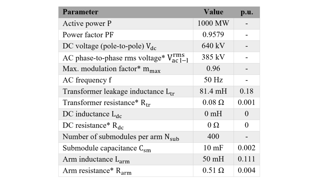
Table I - Parameters of the MMC-HVDC link under study
The used switches in INELFE are also unknown, however, this work considers the IGBT with antiparallel diode FZ1500R33HL3 [27] and the bypass thyristor ACR3200VR33 [28], which are in the good range for being used in the project (see Table II). Finally, Table III gives the parameters concerning the fault management strategy, assuming also realistic values.
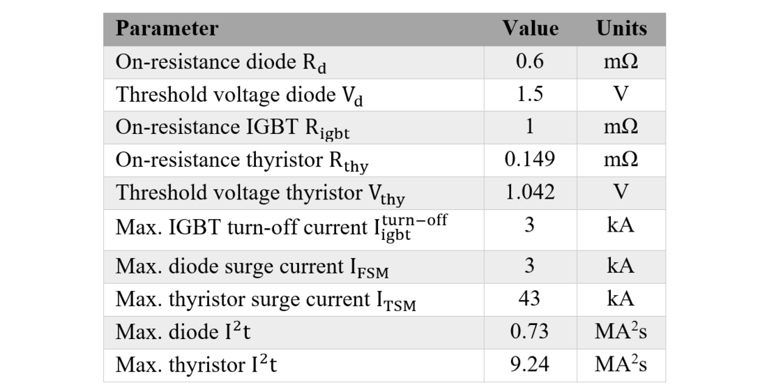
Table II - Parameters of the semiconductors
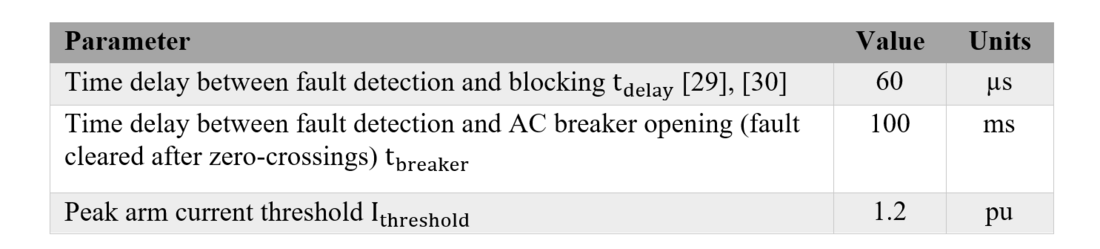
Table III - Parameters of the fault management strategy
Fig. 12 shows the simulation results of the arm currents of Model 2, during the fault process, in which the three fault stages are identified. Fig. 13 shows the first 2 ms of the simulations results in Fig. 12 to illustrate the arm currents during stage 1, before blocking the MMC. As explained before, during stage 1, the arm currents rise with a high di/dt until the blocking of the converter at the beginning of stage 2. Then, the converter enters the rectifier mode of operation, with the currents reaching tens of kA. After the opening of the AC breaker at the beginning of stage 3, the arm currents start to decrease until they reach 0 (inductors in the system discharging).
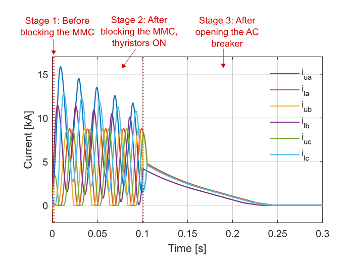
Figure 12 - Simulation results of Model 2: Arm currents during the three stages of the fault
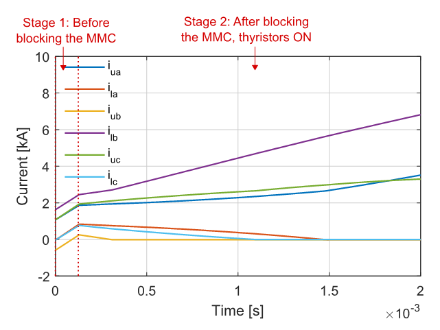
Figure 13 - Simulation results of Model 2: Detail of the arm currents during the stage 1 and the beginning of stage 2
The AC currents and the DC current during the different fault stages are also showed in Fig. 14 and Fig. 15, respectively.
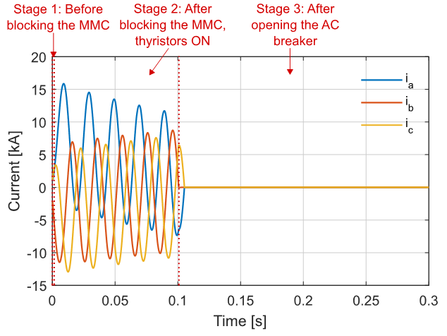
Figure 14 - Simulation results of Model 2: AC currents during the three stages of the fault
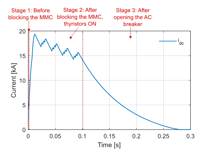
Figure 15 - Simulation results of Model 2: DC current during the three stages of the fault
5.1. Model validation
In this section, the results of a DC fault applied at the MMC terminals of both Model 1 and Model 2 are compared. The results of Model 1 are shown using dotted lines, while the results of Model 2 are depicted in solid lines.
Fig. 16 and Fig. 17 present the part of arm currents circulating through the bypass thyristors and the diodes, respectively, according to their respective on-state resistances and threshold voltages. The results concerning Model 1 come directly from the simulation, where both bypass thyristors and diodes are modelled, while the results of Model 2 are obtained after the offline calculation using the total arm current as input as described in Section 3.2.4. There is a good match between the results of both models, which also validates the simplification taken in Model 2 of modelling only the bypass thyristors and not the diodes in the state-space model during stages 2 and 3. For instance, the highest divergence in the results of the currents through the thyristors is seen in the highest peak of ithy-ua: 13.41 kA for Model 1 and 13.32 for Model 2, leading to an error of 0.7%. It can be seen that thyristors gather most of the fault current compared to the diodes, being the peak current value of 13.4 kA for the thyristors and 2.6 kA for the diodes.
Fig. 18 shows the comparison of the AC currents and Fig. 19 presents the DC current, both illustrating a very similar behaviour.
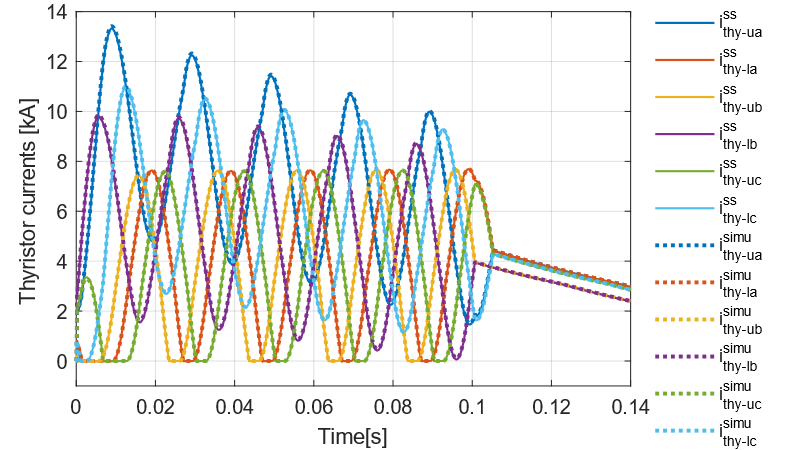
Figure 16 - Simulation results of Model 1 (dotted lines) and 2 (solid lines): Thyristor currents
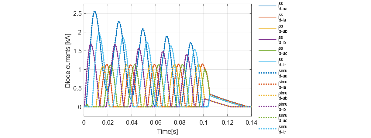
Figure 17 - Simulation results of Model 1 (dotted lines) and 2 (solid lines): Diode currents
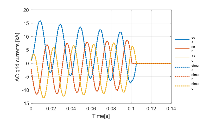
Figure 18 - Simulation results of Model 1 (dotted lines) and 2 (solid lines): AC currents
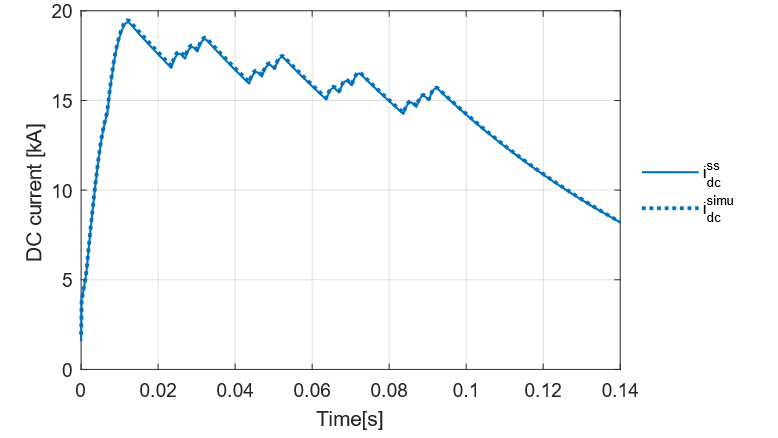
Figure 19 - Simulation results of Model 1 (dotted lines) and 2 (solid lines): DC current
In order to run a simulation of 0.4 s of simulation time in the same computer (IntelCore i5-8250 1.60 GHz 8 GB RAM), Model 1 requires 5 minutes, while Model 2 needs only 7 s.
5.2. Arm inductance results
Before calculating the acceptable range of arm inductance values, Table IV analyses the compliance of Criterion 1 taking into account the project value of 50 mH. The "Ref. values" column shows the maximum admissible values according to the used semiconductors, while the "Simu. values" column presents the values obtained with the simulations of Model 2. It can be seen that all the "Simu. values" are below the ratings of the semiconductors, what leads to the compliance of Criterion 1 and all its subcrtieria. Consequently, the considered IGBT, diode and bypass thyristor are suitable for this application with the assumed parameters.
After applying the methodology described in Section 4, the required minimum value of arm inductance to comply with Criterion 1 is found to be 32 mH. The maximum value of arm inductance that allows to modulate the desired AC waveform and guarantee the PQ provision (Criterion 2) is 117 mH. Then, the acceptable range of arm inductance values that satisfies both criteria is: [32,117] mH. It can be seen that the project value of 50 mH is comprised within the two limits. Then, Table V shows the same analysis as Table IV, but for an arm inductance value of 31 mH, 1 mH lower than the lower limit. It can be seen that C1.4 does not comply, meaning that the diode current exceeds IFSM. It corresponds to the diode current during stage 2 of the fault (since it is different from the IGBT current in C1.1). It is possible to see that the IGBT current during the stage 1 is also close to the limit of 3 kA.
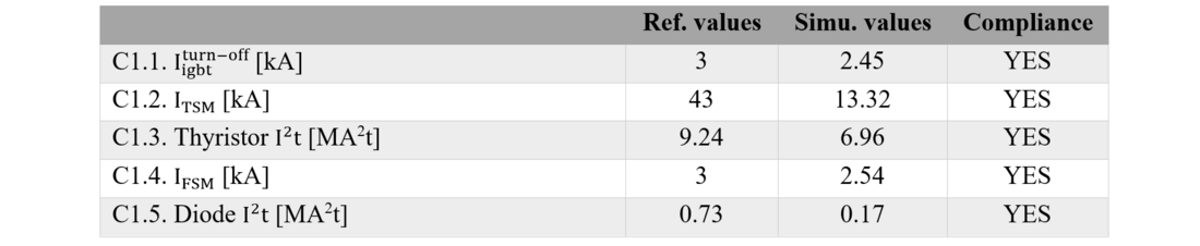
Table IV - Compliance with Criterion 1 considering Larm= 50 mH
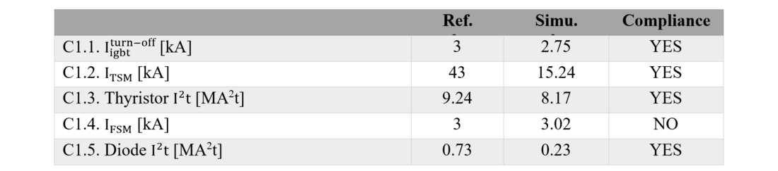
Table V - Compliance with Criterion 1 considering Larm= 31 mH
5.3. Sensitivity analysis
This section analyses the effect that a variation in different parameters have in the compliance of Criterion 1 and 2, thus, in the required value of arm inductance (see Table VI).
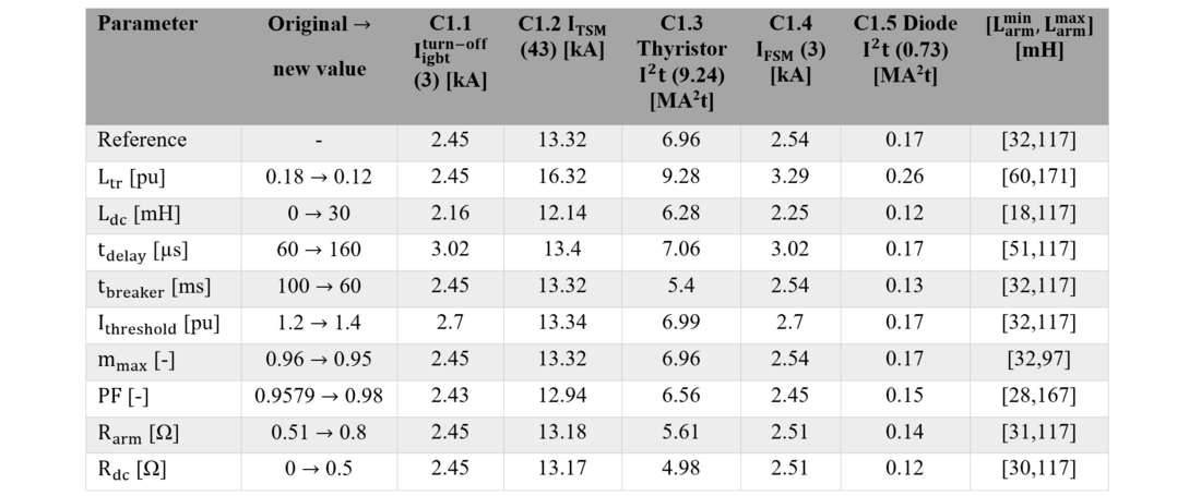
Table VI - Effect of different parameters in the required range of arm inductance (considering Larm= 50 mH)
The first column of Table VI shows the parameter that has been modified with respect to the reference case of section 5 with Larm = 50 mH. The change in the modified parameters is illustrated in the second column, depicting the original and the new value. From the third to the seventh column, the simulation values corresponding to the subcriteria in C1 are presented (the value in the first row between parenthesis being the upper threshold to comply with the given subcriterion). Finally, the last column shows the minimum and maximum value of Larm to comply with C1 and C2, allowing to see the effect of modifying the corresponding parameter.
The first parameter that is modified is the leakage inductance of the transformer Ltr, which is reduced from 0.18 pu to 0.12 pu. This change does not have an effect on C1.1 since it corresponds to the value before the blocking, in which the AC grid contribution to the fault is low. However, the decrease of Ltr has a profound impact in C1.2, C1.3, C1.4 and C1.5, since the peak currents and the l²t that the thyristors and diodes have to withstand are increased. increases as reducing Ltr puts more stress on the diode C1.4, requiring a larger arm inductance.
is increased from 117 mH to 171 mH since the voltage drop across Ltr has decreased, so that Larm can be larger to have the same voltage drop across Lphase.
The effect of adding 30 mH of inductance Ldc in the DC side is also studied. It shows that it can reduce the constraints in all the the subcriteria of C1. Additionally, it does not affect the voltage drop on the AC side, leading to the same , but to a reduced value for the
.
The time delay tdelay between the fault detection (current threshold exceed) and the instant when the submodules are blocked is increased from 60 µs to 160 µs. This clearly increases the constraints on the IGBTs and diodes before the blocking, since the arm currents reach higher values at the end of stage 1 (affecting C1.1 and C1.4). The constraints on C1.2, C1.3 and C1.5, more related to stage 2 and 3, are similar to the reference case. Then, becomes higher and
is kept at the same level.
The time to open the AC breaker tbreaker is reduced from 100 ms to 60 ms. This reduces the duration of stage 2, thus having the same peak current values but lower l²t for the thyristors and diodes, leading to lower constraints for C1.3 and C1.5. Nevertheless, this does not affect neither nor
, which keep the same values.
The effect of increasing the current threshold Ithreshold that assumes the presence of a DC fault affects mainly C1.1 and C1.4, since the current at the time of the blocking is higher, without much affecting the other subcriteria. It could be reduced to have lower constraints on the semiconductors, but then the risk of considering a current transient as a DC fault increases. Considering other criteria for fault detection can be a perspective of this work (e.g. based on the rate of current change di/dt).
The maximum modulation factor mmax is slightly reduced from 0.96 to 0.95. This decreases the margin that the MMC has to modulate the desired AC waveform with the given DC voltage, thus, reducing from 117 mH to 97 mH. C1 is not affected by the change in mmax and
keeps the same reference value.
The nominal power factor PF is changed from 0.9579 to 0.98, meaning that the active power is kept constant but the reactive power is reduced (less apparent power). This leads to a lower current at nominal operation, then slightly decreasing the constraints on the semiconductors, thus, a slightly lower . The effect on
is significant, since less reactive power is transmitted, leading to a reduced AC voltage drop across Lphase. Then, with the same modulation capability, Lphase could be increased, resulting in a higher
.
Finally, the effect of modifying the resistances in the path of the fault is assessed by increasing Rarm and Rdc. The constraints in the semiconductors are reduced for all the subcriteria in C1, except C1.1. The reduction in C1.2 and C1.4 related to the peak current of the switches is quite small, leading to a slightly lower . The effect of increasing both resistances is profound regarding the l²t of the bypass thyristors and the diodes (C1.3 and C1.5). In both cases, increasing the resistance in the fault current path, decreases the time constant of the RL circuit, meaning that the currents reach the steady-state value faster. This reduces the time duration of stages 2 and 3, leading to a lower l²t for both semiconductors. It also points out that the constraints on the switches may be conservative, since any parasitic resistance of the real system that has not been modelled may reduce the real l²t of the semiconductors.
On the one hand, Table VI also shows that for the different parameter modifications, criteria C1.1 and C1.4 are the ones in which the current of the IGBT and the diode, respectively, are closer to the limits. The l²t of the bypass thyristor (C1.3) has more margin, although it is exceeded, for instance, when reducing the leakage inductance of the transformer (for the considered case study the leakage inductance of the transformer is quite high). On the other hand, when analysing C1.2 and C1.5, the calculated values of bypass thyristor peak current and diode l²t, respectively, are pretty far from the limits, outlining that those criteria seem less relevant when defining the arm inductance.
In order to extend the results of Table VI, Fig. 20 and Fig. 21 show different values of Ltr and Ldc and their effect on the range of required values of arm inductance. Fig. 20 shows that increasing Ltr leads to a decrease of since the increase of Ltr ensures the compliance with C1, thus, the safety of the semiconductors. The maximum arm inductance
also decreases since to keep the same voltage drop across Lphase (C2), the increase in the voltage drop across Ltr must be compensated by a reduction of the voltage drop across Larm. Also, Fig. 20 outlines that the acceptable range of arm inductance (vertical distance between
and
) becomes thinner when increasing Ltr.
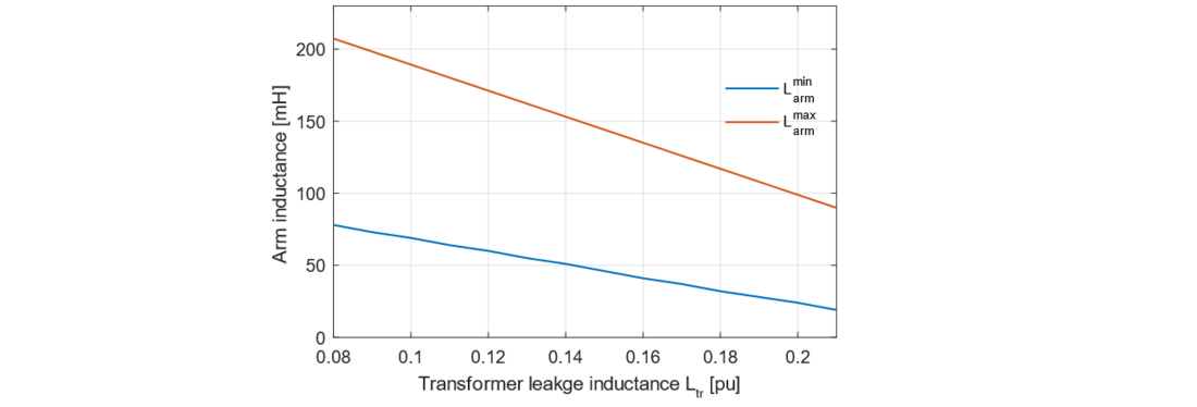
Figure 20 - Minimum and maximum arm inductance as a function of the transformer leakage inductance
Fig. 21 shows that an increase in Ldc also leads to a decrease , as that increase of Ldc guarantees the safety of the semiconductors, thus the minimum value of arm inductance (C1) can be reduced. As it is already introduced in Table VI, the change in Ldc does not impact
(C2).
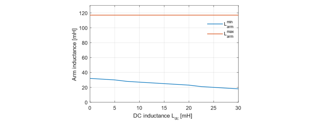
Figure 21 - Minimum and maximum arm inductance as a function of the DC inductance
The variation of the AC voltage is also considered in this analysis, since when designing an HVDC station, their value is a degree of freedom given by the transformer turns ratio. Therefore, Fig. 22 shows the variation between 0.95 pu and 1.05 pu of the nominal AC voltage and their effect on the required range of arm inductance. It can be seen that the change of has a moderate effect on C1. When increasing
,
slightly reduces, since the base impedance becomes higher and for the same pu value, Ltr also increases (requiring less Larm according to C1). This effect compensates the increase in the short-circuit currents due to a higher AC voltage (after Stage 1). The effect on
is profound, increasing
leads to a rapid decrease in the
, since the margin that the MMC has to modulate the desired AC voltage with the given DC voltage becomes lower. It can also be seen that the range of acceptable arm inductances decreases when increasing
. Approximately at
=403 kV,
=
, which represents the maximum AC voltage to comply at the same time with C1 and C2. For greater voltages,
needs to be lower than
, which is not possible. Fig. 22 also points out that a large range of acceptable arm inductances can be reduced by increasing the AC voltage, which would lead to a more interesting point of operation since the nominal AC current of the MMC would be lower (for the same power), leading also to lower losses. Another outcome of Fig. 22 is that voltage fluctuations can have an important impact in the
, meaning that they should be included when applying the methodology to define the acceptable range of arm inductance.
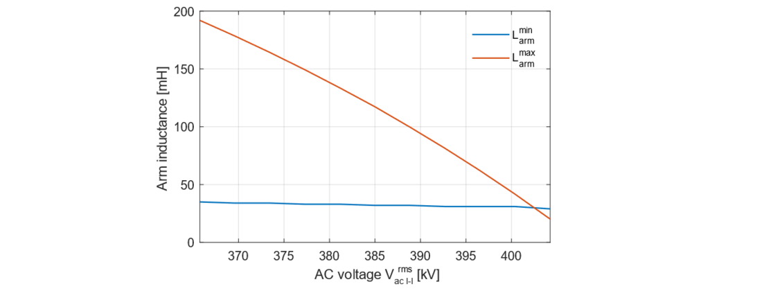
Figure 22 - Minimum and maximum arm inductance as a function of the AC voltage
6. Conclusions
This work presents the methodology to define the arm inductance of a given MMC-HVDC station with fixed AC and DC voltages and based on half-bridge submodules. The methodology gives a range of inductance values that complies at the same time with two criteria, without aiming at providing a full design of an MMC station. Criterion 1 (C1) obtains a minimum value of arm inductance to protect the IGBTs, diodes and bypass thyristors in the submodules from a DC fault. Criterion 2 (C2) calculates a maximum value to ensure the AC voltage drop in the phase inductance allows to provide the desired PQ range with a given DC voltage. The paper details the different stages of a DC pole-to-pole fault, illustrating the different constraints in IGBTs, diodes and bypass thyristors (Criterion 1). A simplified state-space model of an MMC during a DC fault is developed to perform fast simulations. Considering a case study based on a real HVDC link, a DC fault is simulated and the simplified model is validated against a more detailed model. Then, the simplified model is used to obtain the arm inductance range of the MMC-HVDC station, showing its compliance with both criteria. This work presents the effect of modifying different parameters to assess the impact on the stress of each semiconductor and on the required range of arm inductance. For instance, adding DC inductance reduces the constraints in all semiconductors (similarly to adding arm inductance), but without impacting the PQ provision of the converter. Increasing the leakage inductance of the transformer reduces the stress on diodes and bypass thyristors but has a negligible impact on the IGBTs, also it limits the PQ provision of the converter. The time delay during the blocking specially affects the current that the IGBTs have to turn-off, while the time delay of the AC breaker impacts mainly the thermal limit (l²t) of diodes and bypass thyristors. The parasitic resistance in the path of the fault current greatly influences the l²t that diodes and bypass thyristors must handle. The sensitivity analysis also outlined that the IGBT turn-off capability, diode surge current and thyristor l²t are the relevant subcriteria to define the minimum value of inductance for the given case study. However, it has also been shown that the phenomena constraining the minimal value of arm inductance depends on the case study and none of the subcriteria previously highlighted in the literature (diode l²t, IGBT turn-off capability, thyristor surge current) can be used on its own to define the lower limit of inductance for all application cases. Additionally, the AC voltage seen by the converter has a profound effect on the upper limit of arm inductance, highlighting that voltage fluctuations should be considered when applying the methodology.
7. Appendix
The details of the state-space representation of Model 2 in Section 3.2 are given in this appendix. Specifically, the matrixes Aconv, Lconv and Rconv corresponding to Stage 1, 2 and 3 are illustrated. It can be noticed that Aconv and Rconv change for the different stages, but Lconv remains the same.
The matrixes , Lconv,
corresponding to Stage 1 are given in (23), (24), (25), respectively.
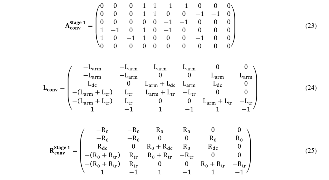
As explained in Section 3.2, during Stage 2 the arm voltage sources are eliminated, the voltage drop of the thyristors is added, and R0 is replaced by R0' (which dynamically changes and takes high values for negative currents independently for each arm). This results in new matrixes and
shown in (26), (27) , respectively.
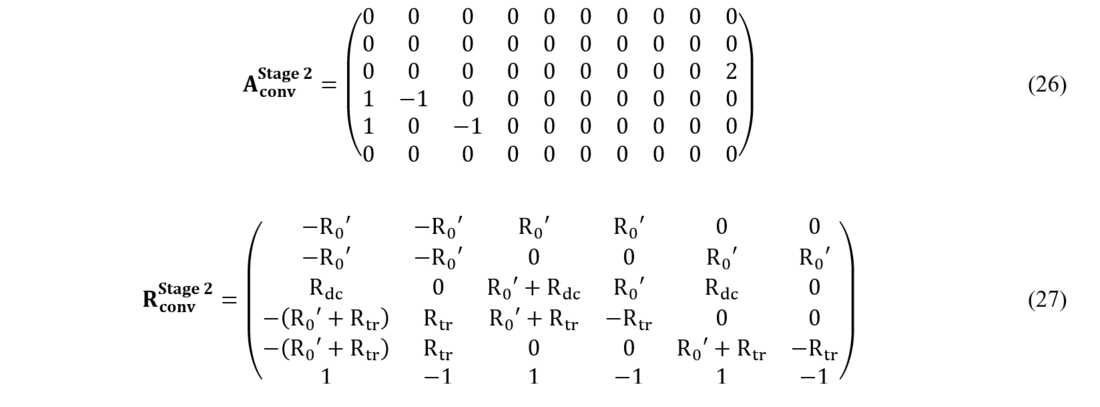
The matrix is initially the same as the matrix in stage 2 (
), but it is dynamically modified when the current of a certain phase goes to zero after the opening of the AC breaker. For example, if it is the current of phase A that goes to 0, the voltage source corresponding to phase A (usa) is changed to 0, which means that the elements of the first column in
become 0. The procedure is analogous if the current of phases B or C go to 0 (second and third column of
, respectively).
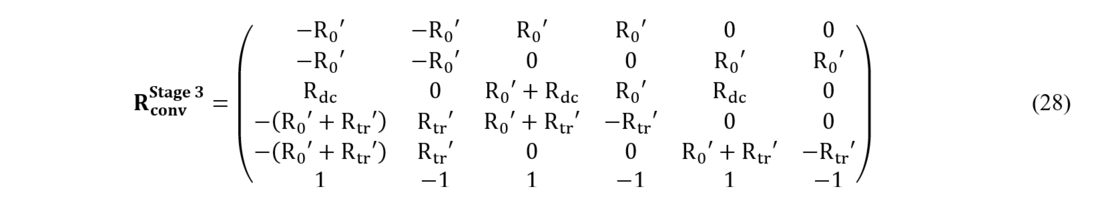
Regarding , which can be seen in (28)), it is analogous to
, in which Rtr has been replaced by Rtr'. Initially Rtr' has the same value than Rtr, but it is dynamically modified when the current of a certain phase goes to 0. The Rtr' corresponding to that phase takes high values to represent the opening of the breaker only for that phase.
Acknowledgment
This work has been supported by a grant overseen by the French National Research Agency (ANR) as part of the "Investissements d’Avenir" Program (ANE-ITE-002-01).
References
- D. Van Hertem, O. Gomis-Bellmunt and J. Liang, HVDC Grids: For Offshore and Supergrid of the Future, IEEE Press Series on Power Engineering. John Wiley & Sons, 2016.
- D. Jovcic and K. Ahmed, High Voltage Direct Current Transmission: Converters, Systems and DC Grids, University of Aberdeen, UK: Wiley, 2015.
- K. Sharifabadi, L. Harnefors, H. P. Nee and S. Norrga, Design, Control, and Application of Modular Multilevel Converters for HVDC Transmission Systems, Wiley-IEEE Press, 2016.
- C. Oates, "Modular Multilevel Converter Design for VSC HVDC Applications," IEEE Journal of Emerging and Selected Topics in Power Electronics, vol. 3, no. 2, pp. 505-515, 2015.
- G. Zhang, Y. Chen, C. Yue, L. Qi and J. Pan, “DC pole-to-pole short-circuit behavior analysis of modular multilevel converter,” in 2014 IEEE Energy Conversion Congress and Exposition (ECCE), Pittsburgh, PA, USA, 2014.
- Z. Xu, H. Xiao, L. Xiao and Z. Zhang, “DC Fault Analysis and Clearance Solutions of MMC-HVDC Systems,” MDPI Energies, vol. 11, no. 4, 2018.
- Y. Zhang, Y. Xu and M. Saeedifard, “Model-Based Design for Reactors of the Modular Multilevel Converter,” IEEE Transactions on Power Electronics, Early Access, 2023, doi: 10.1109/TPEL.2023.3257087.
- B. Li, J. He, J. Tian, Y. Feng and Y. Dong, "DC fault analysis for modular multilevel converter-based system," Journal of Modern Power Systems and Clean Energy, vol. 5, no. 2, pp. 275-282, 2017.
- X. Li, Z. Li, B. Zhao, C. Lu, Q. Song, Y. Zhou, H. Rao, S. Xu and Z. Zhu, “HVdc Reactor Reduction Method Based on Virtual Reactor Fault Current Limiting Control of MMC,” IEEE Transactions on Industrial Electronics, vol. 67, no. 12, pp. 9991-10000, 2020.
- P. Torwelle, A. Bertinato, B. Raison, T. D. Le and M. Petit, "Fault current calculation in MTDC grids considering MMC blocking," Electric Power Systems Research, vol. 207, 2022.
- M. Abedrabbo, W. Leterme and D. Van Hertem, “DC-side fault current estimation approach for HVDC circuit breaker sizing,” Electric Power Systems Research, vol. 212, 2022.
- Y. Wang, W. Wen, C. Zhang, Z. Chen and C. Wang, "Reactor Sizing Criterion for the Continuous Operation of Meshed HB-MMC-Based MTDC System Under DC Faults," IEEE Transactions on Industry Applications, vol. 54, no. 5, pp. 5408-5416, 2018.
- P. Wang, M. Kuschke and K. Strunz, “Analytical Modeling of Modular Multilevel Converter Under Pole-to-Pole DC Fault and Application to System Design and Protection,” IEEE Transactions on Energy Conversion, vol. 37, no. 4, pp. 2722-2736, 2022.
- F. Page, G. Adam, S. Finney, D. Holliday and L. Xu, “DC fault parameter sensitivity analysis,” in 12th IET International Conference on Developments in Power System Protection (DPSP 2014), Copenhagen, Denmark, 2014.
- M. Zygmanowski, B. Grzesik and R. Nalepa, "Capacitance and inductance selection of the modular multilevel converter," in 2013 15th European Conference on Power Electronics and Applications (EPE), 2013, Lille, France.
- K. Ilves, A. Antonopoulos, S. Norrga and H. P. Nee, "Steady-State Analysis of Interaction Between Harmonic Components of Arm and Line Quantities of Modular Multilevel Converters," IEEE Transactions on Power Electronics, vol. 27, no. 1, pp. 57-68, 2012.
- Q. Tu, Z. Xu, H. Huang and J. Zhang, "Parameter design principle of the arm inductor in modular multilevel converter based HVDC," in International Conference on Power System Technology, Hangzhou, China, 2010.
- Y. Li, E. A. Jones and F. Wang, “Circulating Current Suppressing Control’s Impact on Arm Inductance Selection for Modular Multilevel Converter,” IEEE Journal of Emerging and Selected Topics in Power Electronics, vol. 5, no. 1, pp. 182-188, 2017.
- B. Li, Z. Xu., S. Shi, D. Xu and W. Wang, "Comparative Study of the Active and Passive Circulating Current Suppression Methods for Modular Multilevel Converters," IEEE Transactions on Power Electronics, vol. 33, no. 3, pp. 1878-1883, 2018.
- B. Jacobson, P. Karlsson, G. Asplund and L. Harnefors, "VSC - HVDC transmission with cascaded two-level converters," in CIGRE session B4-110, Paris, 2010.
- H. Xiao, Z. Xu and Z. Zhang, "Selection methods of main circuit parameters for modular multilevel converters," IET Renewable Power Generation, vol. 10, no. 6, p. 788–797, 2016.
- R. Li, B. Williams and J. Fletcher, "Influence of Third Harmonic Injection on MMC-based HVDC Transmission Systems," IET Generation, Transmission and Distribution, vol. 10, no. 11, 2016.
- BestPaths, "BestPaths Project," 2018. [Online].
- H. Zhang, D. Jovcic, W. Lin and A. J. Far, “Average value MMC model with accurate blocked state and cell charging/discharging dynamics,” in 4th International Symposium on Environment Friendly Energies and Applications (EFEA), Belgrade, 2016.
- J. D. Paez, DC-DC converters for the interconnection of HVDC grids, PhD dissertation Universite Grenoble Alpes, 2019.
- S. Dennetière, S. Nguefeu, H. Saad and J. Mahseredjian, "Modeling of Modular Multilevel Converters for the France-Spain link," in International Conference on Power Systems Transients (ICPST), Vancouver, Canada, 2013.
- Infineon, "IGBT module FZ1500R33HL3," 2021. [Online].
- Dynex, "Bypass thyristor ACR3200VR33," 2016. [Online].
- Q. Tu, Y. Li, W. Liu, M. Huang, G. Zeng, B. Du and Z. Wu, "Arm Overcurrent Protection and Coordination in MMC-HVDC," in 2018 IEEE Power & Energy Society General Meeting (PESGM), Portland, OR, USA, 2018.
- X. Jiang and M. M. Bakran, "Fault Current Behavior of MMC With the First Blocking Method," IEEE Transactions on Power Electronics, vol. 34, no. 12, pp. 11616-11628, 2019.