Identification of capacitor divider parameters used in CVTs for condition evaluation and future power quality measurement applications
Authors
E. SPERLING, T. BISCHOF - Omicron

Summary
The integration of green energy produced by wind parks or solar farms, the use of new technologies like a vacuum circuit breaker, the increasing number of switching operations and the integration of converter technologies lead to various voltage signals with different frequency contents. The necessity to measure such signals by voltage measurement systems becomes crucial. Ageing processes within the installed asset must be correctly understood before installing filter or protection systems.
Capacitor voltage transformers have been well-established in the grid for several decades. They belong to the conventional instrument transformers class and provide a very small frequency bandwidth characteristic. On the one hand, capacitor voltage dividers are used to divide the high voltage signals into a tap voltage signal of about 10 kV. On the other hand, a pure C-divider belongs to the LPVT type and offers a wideband performance for PQ measurements.
To use CVTs for PQ measurements, it is necessary to determine the primary and secondary capacitor values. This is necessary for a correct design of the additional C3 parameter, which is used for connecting the PQ meter. Another aspect is the evaluation of the health index of the capacitors. The CVD of a CVT is the weakest part. It is now possible to determine capacitor values on-site without dismounting the CVT. A detailed description of the method is provided.
Using the information about the capacitor elements C1 and C2, the paper discusses how the C3 element must be defined and provide a frequency response measurement result of a real CVT in a lab. Based on the findings and the good frequency response behaviour, the paper provides a simulation result to verify the measured behaviour and to identify the impact on the frequency response at the sub-harmonic range. It is shown that several resonances measured at the standard secondary output are not existing when the C3 terminal is used.
For a better orientation, an overview of all the existing voltage measurement systems is provided. The modified CVT with a C3 terminal is included and shows the performance for PQ measurement compared with conventional VTs and LPVTs.
Keywords
CVT, capacitor voltage transformer, PQ, wideband classes, natural resonance, CVD, frequency response behaviour1. Introduction
The existing power grid is within a significant transition period from conventional produced electrical energy towards integration of modern green electrical energy productions. The nature of electric power loads changes from conventional loads towards electronic loads by using semiconductor technologies or various kinds of converter technologies. The integration of electrical green energy and HVDC systems leads to new requirements of the grid topology, increasing numbers of switching operations and significant content of low or high-frequency voltages superimposed to the rated system voltage. Transient overvoltage or long-term overvoltage are additional phenomena that have significant impacts on the installed asset in terms of ageing processes. Due to this fact, it is crucial to integrate information provided by the instrument transformers to receive a current fingerprint of the power system. Based on the findings, several actions are needed to protect the installed asset against forced ageing processes but also keep the system in a stable condition.
One of the very well-known and established voltage measurement systems in high voltage and extra-high voltage grids is the capacitor voltage transformer (CVT), with a base of experience of at least eight decades. First of all, a CVT is a resonance voltage transformer optimised for the rated frequency. But more and more, utilities try to gain experience in PQ measurements by using CVTs as voltage sensors.
On the other hand, the technical committee IEC/TC38, responsible for instrument transformers, is has been published the new standard IEC 61869-1:2023 Edition 2.0. The topic of power quality and the resulting requirements on instrument transformers is introduced for the very first time by WB classes, see Figure 1. [9]
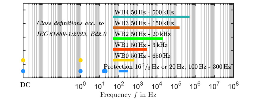
Figure 1 - Wideband class definitions
This paper discusses the possibility of using CVTs for power quality measurements according to the new WB wideband classes. First, a new method will be introduced on how the primary and secondary capacitors of the capacitor divider can be determined without dismounting the CVT unit. The second part focus on the frequency response behaviour of a standard CVT and introduce a portable test unit for measuring the frequency response characteristic of a CVT. The third part presents a solution on how the CVT could be modified for PQ measurements according to WB0 and WB1. The fourth part provides an overview of all the existing voltage measurement systems with their respective frequency response behaviour and includes the modified CVT solution.a
2. Method for determining the single capacitances C1 and C2
The single capacitor elements C1 and C2, without disassembling the capacitor voltage transformer, can be determined by using a method called “CVT-short-circuit-frequency-sweep” (CVT-SCI-f). This method applies two different primary short-circuit impedance tests. The measurement uses a frequency variable AC current source connected to the CVT secondary winding. The resulting voltages and currents are measured. [2]
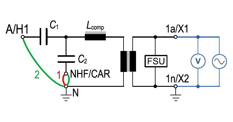
Figure 2 - Measurement setup for first test ZSC1 (red) and second test ZSC2 (green) [2]
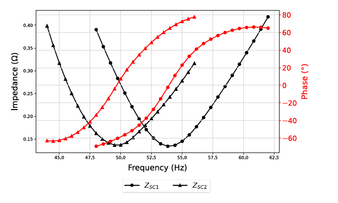
Figure 3 - Typical short-circuit impedance curves of a CVT [2]
The first test contains the capacitor C2 and measures the frequency-dependent short-circuit impedance ZSC1 using the red wiring. A second test, see green wiring, contains the capacitors C1 and C2 and measures the frequency-dependent short-circuit impedance ZSC2, see Figure 2. Typical frequencydependent short-circuit impedance curves of CVTs are shown in Figure 3. The black-coloured curve with the bullet corresponds to ZSC1 , and that with the diamond to ZSC2. Both red curves are the corresponding phase information. The short-circuit impedance ZSC1 curve shows a series resonance circuit with C2 and the total inductance Ltot, whereas the short-circuit impedance ZSC2 shows a resonance circuit with Ctot (C1 parallel to C2 ) and Ltot. The total inductance includes the compensation coil of the CVT and the stray inductance of the intermediate voltage transformer (IVT).
From the curves ZSC1 and ZSC2, the resonance frequency is determined at the phase response of 0°, which is used to calculate the capacitances C1 and Ctot. [2]
The calculation of ,
and
referred to IVT secondary side uses the following formulas: [2]
Equation 1
Equation 2
Equation 3
The capacitance and
are transformed to the IVT primary side with the following formula: [2]
Equation 4
Equation 5
Equation 6
The resultant capacitance Cr from and
is calculated using Equation 6. [2]
Further, it was shown that consecutively measurements obtained by the CVT-SCI-f method on the same CVT resulted in repeatable values. The coefficient of variation (CV) is typically 0.05 %. The measured capacitances determined with the CVT-SCI-f method are compared to reference values. For the comparison, the percentage capacitance deviation PCD is introduced. [2]
Equation 7
As a reference value, the measured capacitance at high voltage or the rated capacitance of the CVT can be used. The rated capacitance values C1 , C2 and Cr are stated on the CVT rating plate. The tolerance of the capacitance values is specified with - 5 % to + 10 % as per standard IEC [3].
In Figure 4, the paper [2] investigated 14 different CVTs and compared the PCD result of the CVT-SCI-f method with the factory acceptance test C1meas and C2meas at high voltage (light blue and light green) and to the rated capacitance values C1r and C2r stated on the rating plate (dark blue and dark green).
The PCD generally smaller than 3 %. The comparison with the factory acceptance test at high voltages shows a PCD value below 2 %. Thus, the CVT-SCI-f method can be used for condition assessment and in-depth diagnostic of the capacitor voltage divider.
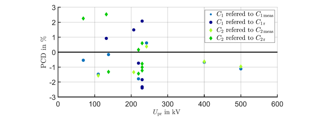
Figure 4 - C1 and C2 error distribution of PCD on different CVTs and voltage levels [2]
3. Condition evaluation
A capacitor unit consists of several identical single capacitor elements connected in series. Depending on the rated voltage, several capacitor units are connected in series. By rule of thumb, the number of single elements corresponds to Equation 8 and reflects a typical voltage drop of Uelem ≈ 0.85 kV at rated primary voltage Upr [5]. The number of single elements can be estimated using Equation 8 [5]. The voltage of a single capacitance element Uelem can be determined with the relation between Upr and the total number of elements ntotal using Equation 9. The capacitive ratio KC is described in the following Equation 10 [3].
Equation 8
Equation 9
Equation 10
The capacitance value C1 is lower than the capacitance value C2 . Thus, a defect of a capacitive element in capacitor C1 has less influence on the voltage ratio error than a defect element in capacitor C2 .
A defect in capacitor C1 moves the voltage ratio error to positive values. For CVTs (e.g. 72.5 kV) the effect is higher than for CVTs (e.g. 550 kV). There is no significant change in the phase displacement observed. In addition, it was proved that the influence of shorted capacitor elements is linear. The capacitor ratio KC decreases slightly with shorted elements in capacitor C1 . [5]
In case of a defect within the capacitor C2 , the voltage ratio error is shifted towards negative values. The sensitivity of the effect does not depend on the voltage level. There is a significant impact on the phase displacement of the CVT. The capacitive ratio KC increases more significantly in the case of shorted elements in capacitor C2 . [5]
4. Standard CVT bandwidth performance
The equivalent circuit diagram of a CVT is illustrated in Figure 5. CVTs can be characterised as a resonance transformer precision optimised at the rated frequency of the system. The corresponding vector diagram is shown in Figure 6. For more information on how to develop and read the vector diagram, see Figure 6 [4]. As indicated in the figure, the CVT consists of four main elements, such as the capacitor voltage divider (CVD), a compensation coil, an MV-VT and a Ferro-resonance suppression unit (FSU).
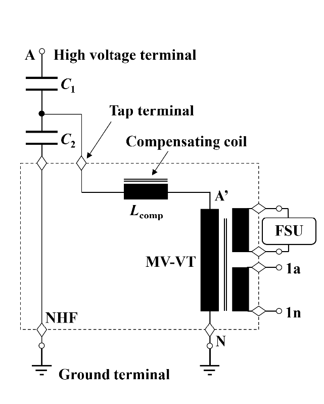
Figure 5 - ECD of a CVT
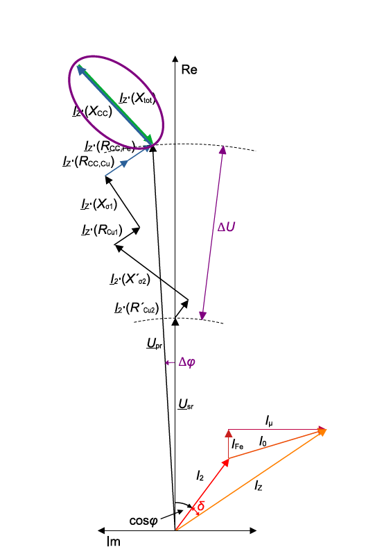
Figure 6 - Vector diagram of a CVT
- The capacitor voltage divider is used to divide the primary voltage Upr to a step voltage level Utap in a range from 8 kV to 14 kV.
- The compensation coil is needed to compensate the resulting impact of the CVD to the total accuracy by using the Thomson equation, see Equation 11. Figure 6 shows the compensation of the capacitor pointer with the compensation coil pointer, marked with a purple oval. The base for compensation is the rated frequency fr of the system, mainly 50 Hz or 60 Hz.
Equation 11
- The MV voltage instrument transformer transforms the Utap down to the rated secondary voltage Usr.
- The Ferro-resonance suppression unit (FSU) is needed to protect the CVT against single-phase Ferro-resonance oscillations and shall be checked as a routine test according to IEC 61869-5.
Various damping circuit solutions are on the market, which can be split into three main categories, such as resonance passive damping, passive damping, and active damping systems, using electronic components see Table 1. Many other FSU solutions are also on the market and actively used for CVT protection. The focus of all the solutions is on the sub-harmonic frequency range at fr/3, fr/5 and fr/7 levels. Ferro-resonance oscillation can only be damped when high resistive consumptions are available.
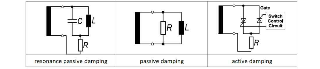
Table 1 - Examples of damping systems
5. Test setup
The measurement of the frequency response behaviour was carried out according to the principal test setup shown in Figure 7. The test voltage signal is generated by a Franeo100 unit with 10 V(p-p) and is applied to the primary terminal, illustrated with a yellow cable. The primary voltage, red cable, and the secondary voltage, blue cable, are used for measuring the voltage at the standard terminals A-N and 1a-1n.
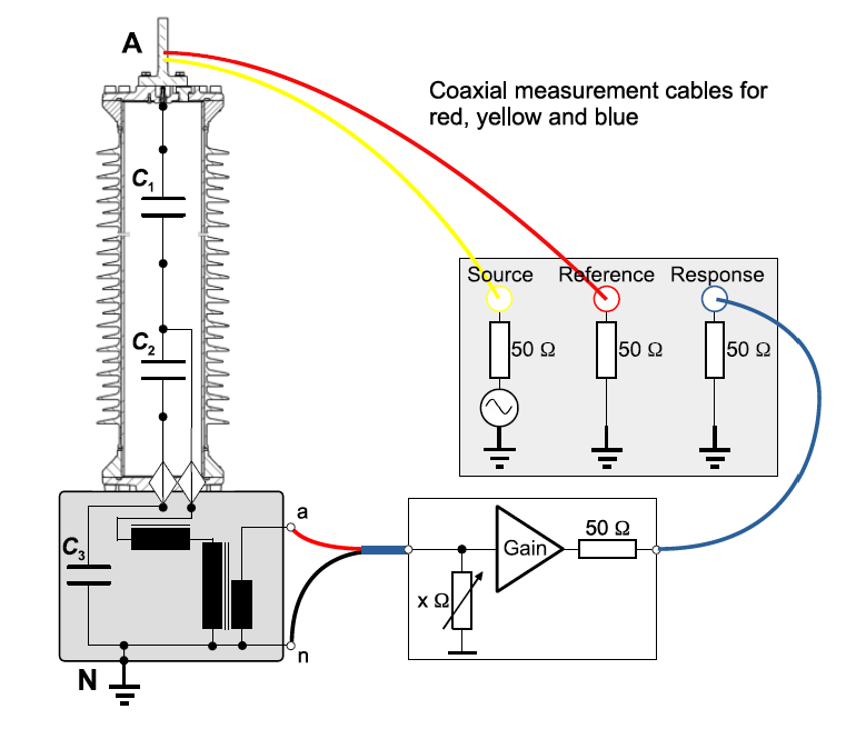
Figure 7 - Principal test setup
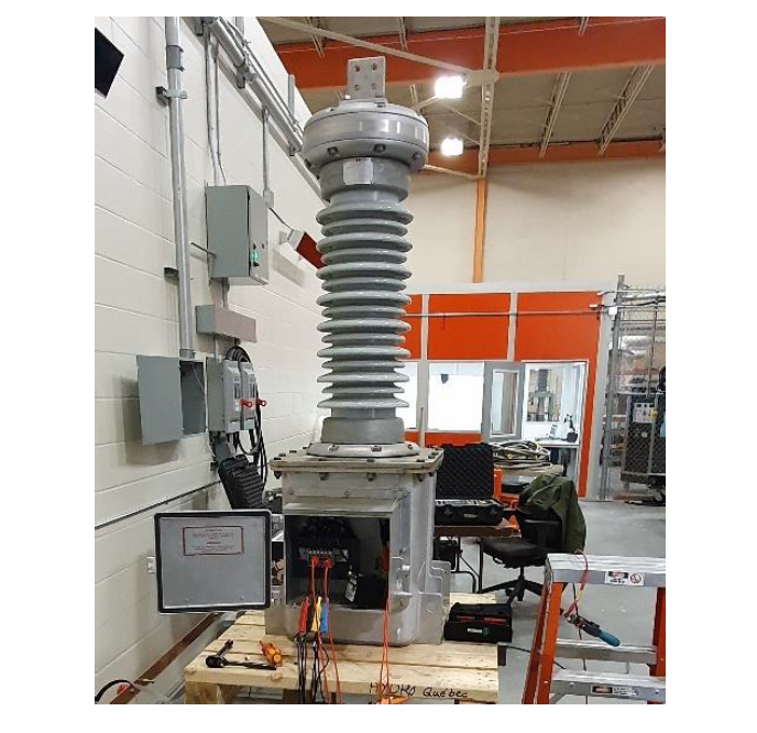
Figure 8 - Test setup with unit under test
For a correct burden value, an electronic impedance converter is used between the secondary output terminals and the measurement unit. The value of connected burden has an impact on the frequency response behaviour and must be considered, especially for LPITs. For this measurement, the CVT was in no-load condition to neglect the negative impact on the frequency response behaviour. The input impedance of the PQ meter with 1 MΩ was connected. The measurement systems analyse the secondary and primary voltage levels and provide the ratio error εU in per cent and the phase displacement Δφ in minutes or degrees according to the standard IEC 61869-1 and its relevant subparts.
6. Measurement results
As indicated in the chapter above, the test voltage level to measure the frequency response characteristic was 10 V(p-p), which is very low compared with the rated voltage level. Nevertheless, when using the relative application bandwidth and adapting the values for rated frequency of 60 Hz, the frequency response behaviour is not affected. A vertical shift for the voltage error ΔεU ( fr ), based on εU ( fr ) with the same frequency, is the consequence.
Detailed information can be found in [11].
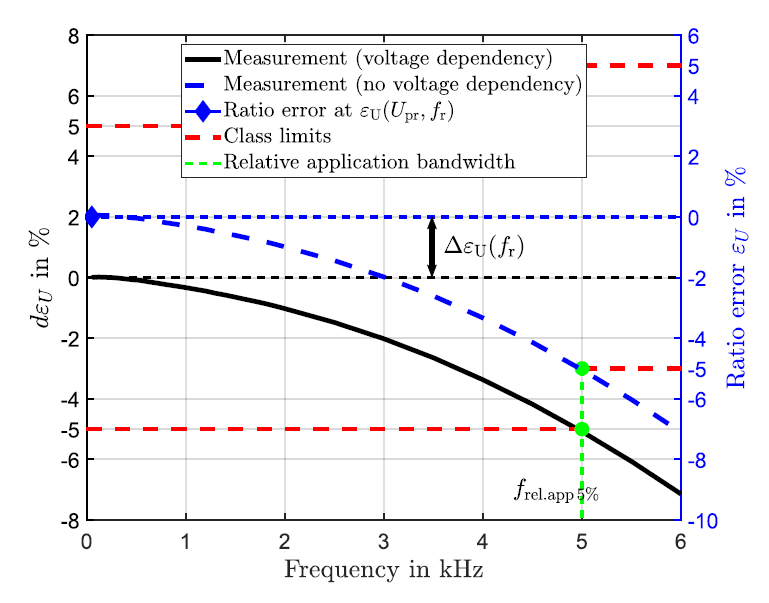
Figure 9 - Definition of relative application bandwidth
Figure 10 shows a frequency response measurement of a CVT from 10 Hz up to 30 kHz for a 72.5 kV system voltage. Figure 11 provides a detailed picture from 10 Hz to 3 kHz for better visualisation.
In Figure 10, the blue curve represents the ratio error εU and the green curve that of the corresponding phase displacement Δφ. Several significant resonance peaks can be determined, for example, at 30 Hz, 400 Hz, 3.5 kHz, 12 kHz and at 17 kHz. All the resonances depend on various stray capacitances and significant inductive elements provided by the compensation coil, main MV-transformers, and also on FSU type. The measurement results show clearly that a standard CVT cannot be used for PQ measurements when using the standard secondary output terminals.
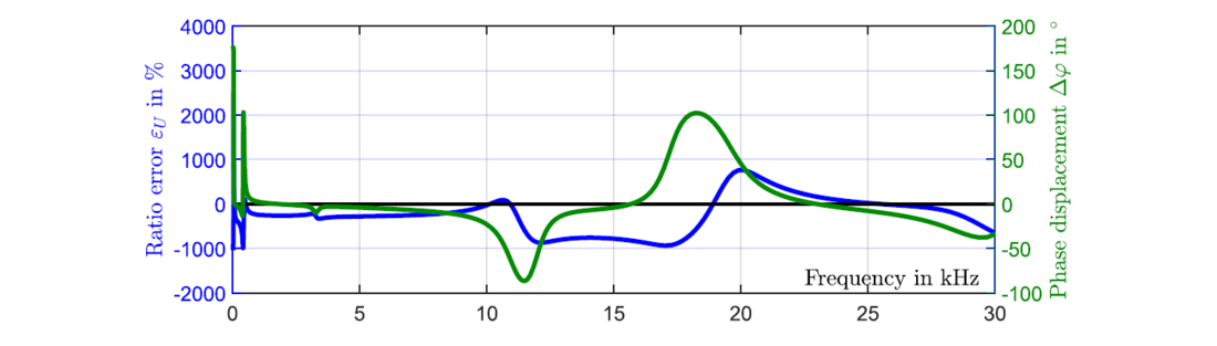
Figure 10 - Frequency response result of a CVT up to 30kHz
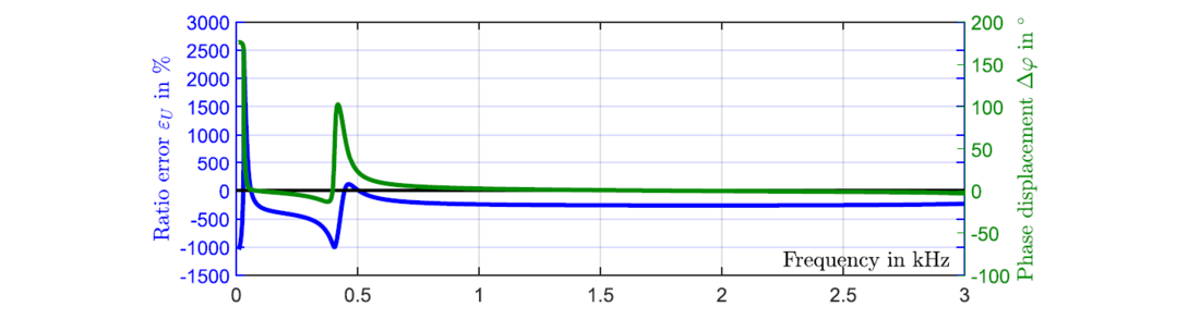
Figure 11 - Frequency response up to 3kHz based on Figure 10
The resonance peaks in Figure 11 are linked to the main inductance of the MV-VT at 30 Hz, and the second resonance peak at 400 Hz depends on the compensation coil inductance. From approximately 1 kHz to 3 kHz, the response curve shows a nearly linear behaviour.
7. CVT modification for PQ measurements
As described in the previous chapters, the CVT consists of a CVD, which divides the high voltage potential down to a tap voltage level. This voltage level is optimized for the MV-VT to connect highburden values for high-precision standard classes. As described in the previous chapter, the voltage level is typically in the range of 8 kV to 14 kV.
Another solution is needed to reduce the voltage level down to 100 V or lower for a direct PQ measurement system. One possible solution is to place additional capacitor C3 between the foot-point
of the secondary capacitor C2 and ground N. Depending on the values of C1, C2 and the required PQ voltage U3, C3 can be calculated by using the following formula. [10]
Equation 12
For the test object, the values are for U1 = 40.25 kV (p-g), C1 = 14690 pF, C2 = 39095 pF, C3 = 12 μF and lead to a voltage level of U3 = 35.78 V. When the capacitance C3 is installed at the manufacture place, the adjustment and later accuracy measurements include the impact. When C3 is installed later onsite, the resulting voltage error depends on the used C3 value. For this test object, the difference of the CVD ratio KC is 0.2366 %, with and without C3, which can be measured on the secondary voltage level and must be considered.
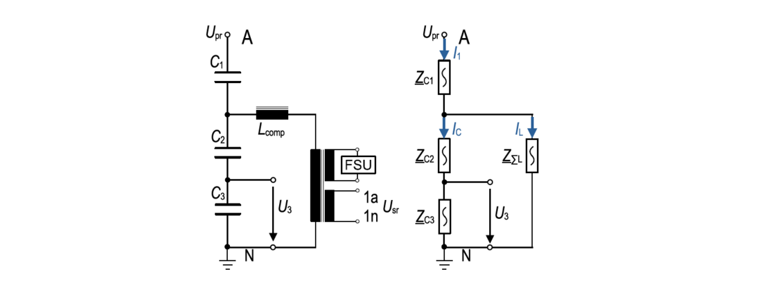
Figure 12 - CVT ECD, left: with elements, right: impedance view
Figure 12, on the left side, shows the equivalent circuit diagram with additional capacitor C3. The circuit diagram on the right side of the same figure shows the impedance view. The impedance ?ΣL represents the inductance of the MV-VT, in parallel connection with the inductance of the FSU and connected in series with the inductance of the compensation coil. With increasing frequency, the current IC increase linearly, and the current IL decrease linearly. In principle, as lower the current IL, as lower the impact on U3. This fact leads to a no-load condition of the CVT or to a high impedance value provided by electronic metering and protection systems. The level of no-load current for magnetising the main iron core is impressed and depends on voltage level and frequency and cannot be easily changed.
8. Measurement result
Figure 13 shows the measurement result using the C3 capacitor voltage drop under the no-load condition of the CVT. From 0.2 kHz up to 3 kHz, the voltage error, see the blue curve, is very stable and could be used for PQ measurements. Further measurements, up to 20 kHz, show similar behaviour. Below 0.2 kHz, the system is not linear enough to provide the required accuracy classes definitions WB0 to WB1 of the new standard IEC 61869-1 Edition 2.0. The first resonance point at 30 Hz is still dependent on the main inductance of the MV-VT.
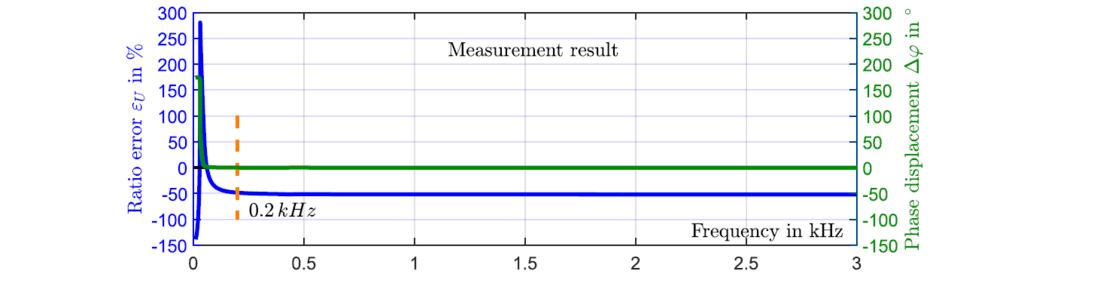
Figure 13 - Frequency response measurement at C3 terminal of a CVT
9. Simulation result
Using the equivalent circuit diagram of Figure 12 and the capacitor elements C1, C2, C3, and the resulting inductance Lcomp, as well as approximated LMV-VT and LFSU, the network simulator program LTspice was used to understand the dependency of all the elements. Especially the question was: Is it possible to pre-calculate the frequency response behaviour and compare it with the measured results in Figure 13? The following vales are used: C1 = 14690 pF, C2 = 39095 pF, C3 = 12 μF, Lcomp = 130.82 H, LMV-VT = 8000 H, LFSU = 420 H. Resistive components are not considered!
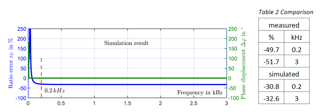
Figure 14 - Simulation result of the frequency response behaviour
The result of the simulation in Figure 14 and compared with the measured results in Figure 13 shows the same behaviour and a good match. Due to not considering resistive elements, a difference in
amplitude values is comprehensible. The number of resonance points and the position at the frequency axis is not affected, which is reasonable. The difference between measured and simulated
results of the ratio error (blue curves) is shown in Table 2. As mentioned above, precise the circuit will solve the deviation.
10. Comparisons of modified CVTs and other voltage measurement systems
The performance for the measurement of frequency signals between DC and impulse voltages of conventional VTs, CVTs and LPVTs is discussed in TR IEC 61869-103 and in CIGRE TB 814. At the CIGRE A3 committee, a working group A3.45 work on specific questions on how voltage measuring systems can be evaluated and characterised depending on various applications. [7][8]
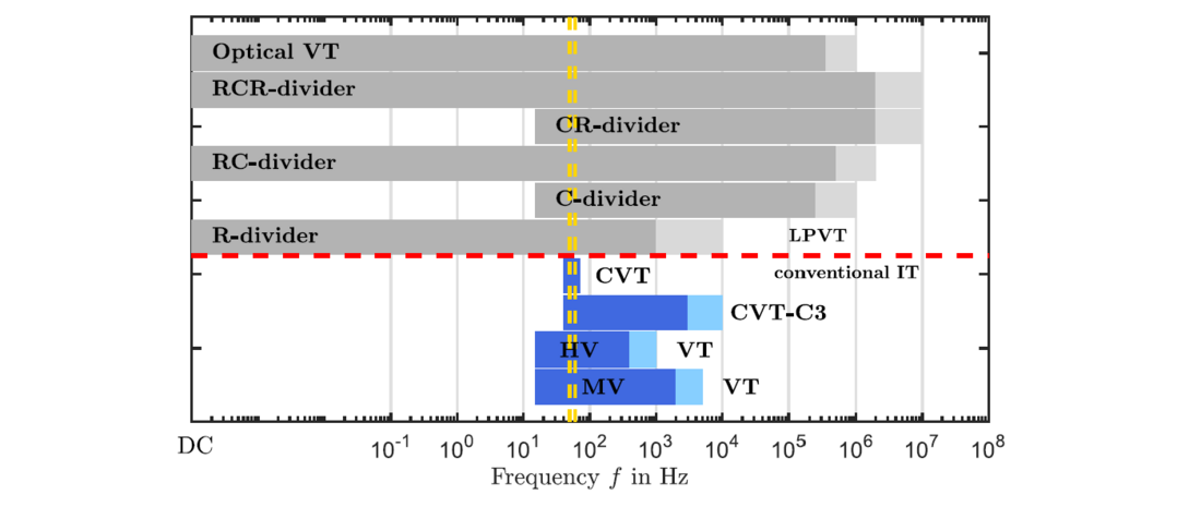
Figure 15 - Voltage measurement systems and their frequency response behaviour
An overview of all existing voltage measurement technologies is illustrated in Figure 15. Above the reddotted line, all the LPVT solutions are listed. Depending on the internal design, it is possible to measure voltage signals from DC to very high frequencies or transient voltage signals. Below the red-dotted line, both conventional technologies are listed. The dark colours represent typical bandwidth, and the light colours that of various bandwidth performances depending on system voltage level and IT design. The modified CVT-C3, compared to the standard CVT above, illustrates impressively that the CVD of the CVT can be used for a wider frequency bandwidth and could meet the new class WB1 or maybe in the future also the WB2 class, see Figure 1. [9]
Conclusion
Capacitor voltage transformers for voltage measurements are well established in high-voltage and extra-high voltage grids for decades. It is shown that a value identification of the capacitor elements C1 and C2 can be performed on-site without dismounting the CVT unit with high precision. Based on the results, it is possible to evaluate the health index of a CVD and use the findings for on-site modification by placing a C3 at the foot point of the CVD. Frequency response measurements on a standard CVT and on a modified CVT show that a standard CVT cannot be used for PQ measurements due to the presence of several resonance points. The modified CVT solution can offer PQ measurements from approximately 200 Hz up to 3 kHz. A higher frequency bandwidth might be possible. As an outlook, it is necessary to check the impact on the frequency response characteristic of C3 by varying burden values connected to the standard secondary terminals. A correlation between the connected burden and its value and the impact on the transfer characteristic of the CVT could be very helpful for installed CVTs but also for new CVTs.
Finally, an overview provides all the existing voltage measurement systems, which can be used for a first evaluation of which measurement system provides the required performance for PQ measurements depending on the application. Today, the product standard IEC 61869-5 Edition 1.0 does not provide any information about the topic of high-frequency measurements. It would be helpful if the new Edition 2.0 provide detailed information on how PQ measurement applications must be considered.
References
- SC A3, CIGRE TB 394: “State of the art of instrument transformers”, CIGRE, October 2009.
- Thomas Bischof, David Gopp, Dmitry Atlas, “A new method for determining the C-divider capacitances of a Capacitor Voltage Transformer with frequency measurements”, IEEE PES GTD – Futuring the Power Grid, Istanbul, 2023
- IEC 61869-5, “IEC 61869-5:2011 Instrument transformers, Part 5: Additional requirements for capacitor voltage transformers.” OVE Austrian Electrotechnical Association, Jan. 06, 2012.
- M. Freiburg, E. Sperling, F. Predl, “Capacitive Voltage Transformers – Electrical Performance and Effective Diagnostic Measures”, CMD 2016 (Condition Monitoring and Diagnosis 2016), 25.9.-28.9.2016, Xi'an, China
- IEC 61869-1 “Instrument transformers – Part 1: General requirements”, Edition 1.0, 2007-10
- IEC 60358-1, “Coupling capacitors and capacitor dividers – Part 1: General rules”, Edition 1.0, 2012-06
- SC B3, CIGRE TB 814: “LPIT applications in HV Gas Insulated Switchgear”, CIGRE, Sept. 2020
- IEC/TR 61869-103: Edition 1.0, 2012-05, “Instrument transformers – The use of instrument transformers for power quality measurement”
- IEC 61869-1:2023: “Instrument transformers – Part 1: General requirements”, Edition 2.0
- M. Yazdani, J. Rickmann, D. Fredrich, “Innovative Applications of High Voltage Instrument Transformers for Monitoring Power System Transients and Harmonics”, CIGRE-435, CIGRE Canada Conference & Expo, Toronto October 25-28, 2021
- E. Sperling, M. Freiburg, D. Gopp, “Assessment of high frequency performance of voltage instrument transformers using the relative application bandwidth”, VDE - Hochspannungs-technik 2022, 8.11.-10.11.2022, Berlin, Germany